TPS7A39
ZHCSGP0A –JULY 2017–REVISED SEPTEMBER 2017
www.ti.com.cn
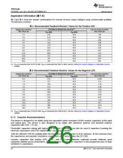
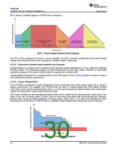
图 67 shows a simplified diagram of PSRR versus frequency.
Bandgap RC
Filter
Error Amplifier, Flat-Gain
Region
Error Amplifier,
Gain Roll-off
Output Capacitor
|ZCOUT| Decreasing
Output Capacitor
|ZCOUT| Increasing
Bandgap
10 Hz œ 1 MHz
Sub 10 Hz
100 kHz +
Frequency (Hz)
图 67. Power-Supply Rejection Ratio Diagram
An LDO is often employed not only as a dc-dc regulator, but also to provide exceptionally clean power-supply
voltages that exhibit ultra-low noise and ripple to sensitive system components.
8.1.9.2 Channel-to-Channel Output Isolation and Crosstalk
Output isolation is a measure of how well the device prevents voltage disturbances on one output from affecting
the other output. This attenuation appears in load transient tests on the other output; however, to numerically
quantify the rejection, the output channel isolation is expressed in decibels (dB).
Output isolation performance is a strong function of the PCB layout. See the Layout Guidelines section on how to
best optimize the isolation performance.
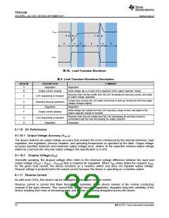
8.1.9.3 Output Voltage Noise
The TPS7A39 is designed for system applications where minimizing noise on the power-supply rail is critical to
system performance. For example, the TPS7A39 can be used in a phase-locked loop (PLL)-based clocking
circuit that can be used for minimum phase noise, or in test and measurement systems where even small power-
supply noise fluctuations reduce system dynamic range.
LDO noise is defined as the internally-generated intrinsic noise created by the semiconductor circuits alone. This
noise is the sum of various types of noise (such as shot noise associated with current-through-pin junctions,
thermal noise caused by thermal agitation of charge carriers, flicker noise, or 1/f noise and dominates at lower
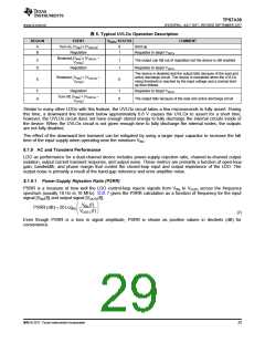
frequencies as a function of 1/f). 图 68 shows a simplified output voltage noise density plot versus frequency.
Wide-band Noise
Integrated Noise
From Bandgap and Error Amplifier
Measurement Noise Floor
Frequency (Hz)
图 68. Output Voltage Noise Diagram
30
版权 © 2017, Texas Instruments Incorporated

 TI [ TEXAS INSTRUMENTS ]