TPS7A39
ZHCSGP0A –JULY 2017–REVISED SEPTEMBER 2017
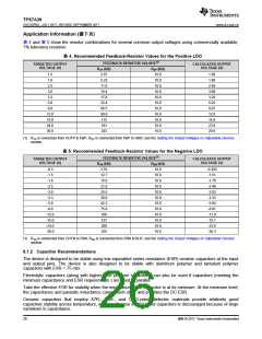
www.ti.com.cn
Feature Description (接下页)
7.3.4.1 Start-Up Tracking
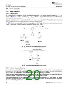
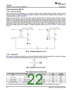
图 63 shows how both regulators use a common reference, which enables start-up tracking. Using the same
reference voltage for both the positive and negative regulators ensures that the regulators start-up together in a
controlled fashion; see 图 24 and 图 25.
Ramps on VINx with EN = VINP that are slower than the soft-start time do not have start-up tracking. If ramps
slower than the soft-start time are used then enable should be used to start the device to ensure start-up
tracking. A small mismatch between the positive and negative internal enable thresholds means that one channel
turns on at a slightly lower input voltage than the other channel. This mismatch is typically not a problem in most
applications and is easily solved by controlling the start-up with enable. The external signal can come from the
input power supply power-good indicator, a voltage supervisor output such as the TPS3701, or from another
source.
VOUTN = VBUF × (-R1N/R2N
)
VOUTP = VNR/SS × (1+R1P/R2P
)
VINN
VINP
R1N
R1P
VNR/SS
GND
R2N
R2P
GND
VBUF
x1
图 63. Simplified Regulation Circuit
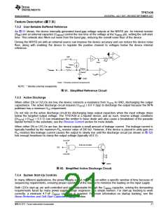
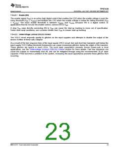
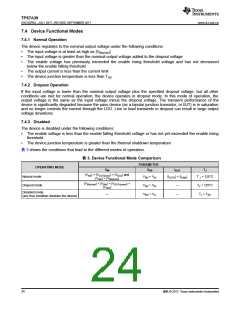
7.3.4.2 Sequencing
图 64 and 表 2 describe how the turn-on and turn-off times of both LDOs (respectively) is controlled by setting
the enable circuit (EN) and undervoltage lockout circuit (UVLOP and UVLON).
UVLOP
Internal
Enable
EN
UVLON
图 64. Simplified Turn-On Control
表 2. Sequencing Functionality Table
POSITIVE INPUT VOLTAGE NEGATIVE INPUT VOLTAGE
(VINP (VINN
LDO
STATUS
ACTIVE
DISCHARGE
ENABLE STATUS
)
)
EN = 1
On
Off
Off
Off
Off
Off
VINP ≥ VUVLOP
VINN ≤ VUVLON
EN = 0
On(1)
On(1)
On(1)
On(1)
VINP ≥ VUVLOP
VINP < VUVLOP
VINN > VUVLON
INN ≤ VUVLON
VINN > VUVLON – VHYSN
EN = don't care
EN = don't care
EN = don't care
V
VINP < VUVLOP – VHYSP
(1) The active discharge remains on as long as VINx and VOUTx provide enough headroom for the discharge circuit to function.
22
版权 © 2017, Texas Instruments Incorporated

 TI [ TEXAS INSTRUMENTS ]