TPS7A39
ZHCSGP0A –JULY 2017–REVISED SEPTEMBER 2017
www.ti.com.cn
7.3 Feature Description
7.3.1 Voltage Regulation
7.3.1.1 DC Regulation
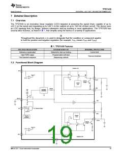
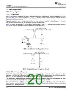
An LDO functions as a buffered op-amp in which the input signal is the internal reference voltage (VNR/SS), as
shown in 图 59, and in normal regulation VFBP = VNR/SS. Sharing a single reference ensures that both channels
track each other during start-up.
VNR/SS is designed to have a very low-bandwidth at the input to the error amplifier through the use of a low-pass
filter. As such, the reference can be considered as a pure dc input signal.
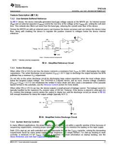
As 图 60 shows, the negative LDO on the device regulates with a VFBN = 0 V and inverts the positive reference
(VBUF). This topology allows the negative regulator to regulate down to 0 V.
VOUTP = VNR/SS × (1+R1P/R2P
)
VINP
To Load
R1P
NR/SS
VFBP
R2P
CNR/SS
GND
Bandgap
GND
Reference
GND
图 59. Simplified Positive Regulation Circuit
VOUTN = VBUF × (-R1N/R2N
)
VINN
To Load
R1N
VFBN
GND
R2N
VBUF
图 60. Simplified Negative Regulation Circuit
7.3.1.2 AC and Transient Response
Each LDO responds quickly to a transient on the input supply (line transient) or the output current (load
transient). This LDO has a high power-supply rejection ratio (PSRR) and, when coupled with a low internal noise-
floor (Vn), the LDO approximates an ideal power supply in ac and large-signal conditions.
The performance and internal layout of the device minimizes the coupling of noise from one channel to the other
channel (crosstalk). Good printed circuit board (PCB) layout minimizes the crosstalk.
The noise-reduction and soft-start capacitor (CNR/SS) and feed-forward capacitor (CFFx) easily reduce the device
noise floor and improve PSRR; see the Optimizing Noise and PSRR section for more information on optimizing
the noise and PSRR performance.
20
版权 © 2017, Texas Instruments Incorporated

 TI [ TEXAS INSTRUMENTS ]