TPS7A39
www.ti.com.cn
ZHCSGP0A –JULY 2017–REVISED SEPTEMBER 2017
Feature Description (接下页)
7.3.2 User-Settable Buffered Reference
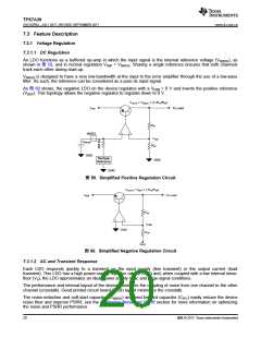
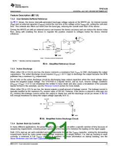
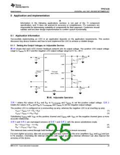
As 图 61 shows, the device internally generated band-gap voltage outputs at the NR/SS pin. An internal resistor
(RNR) and an external capacitor (CNR/SS) control the rise time of the voltage at the VNR/SS pin, setting the soft-start
time. This network also filters out noise from the band gap, reducing the overall noise floor of the device.
Driving the NR/SS pin with an external source can improve the device accuracy and can reduce the device noise
floor, along with enabling the device to regulate the positive channel to voltages below the device internal
reference.
+
SW
VFBN
œ
x1
R2N*
VBUF
INR/SS
RNR/SS
VNR/SS
CNR/SS
VBandgap
+
*
œ
VFBP
GND
Note: * Denotes external components
NOTE: * denotes external components.
图 61. Simplified Reference Circuit
7.3.3 Active Discharge
When either EN or UVLOx are low, the device connects a resistance from VOUTx to GND, discharging the output
capacitance. The active discharge circuit requires |VOUTx| ≥ 0.6 V (typ) to discharge the output because the NPN
pulldown has a minimum VCE requirement.
Do not rely on the active discharge circuit for discharging large output capacitors when the input voltage drops
below the targeted output voltage. The TPS7A39 is a bipolar device, and as such, reverse voltage conditions
(|VOUTx| ≥ |VINX| + 0.3 V) can breakdown the emitter to base diode and also cause a breakdown of the parasitic
bipolar formed in the substrate; see the Reverse Current section for more details.
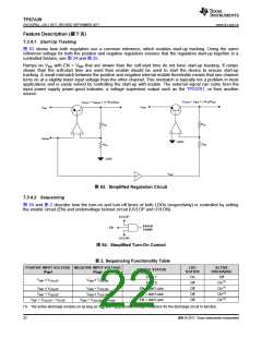
When either EN or UVLOx are low, the device outputs a small amount of leakage current. The leakage current is
typically handled by the maximum R2x resistor value of 240 kΩ. However, if the device is placed in unity gain (no
R2x resistor) this leakage current causes the output to slowly rise until the discharge circuit (as shown in 图 62)
has enough headroom to clamp the output voltage (typically ±0.6 V).
UVLOP
Internal Enable
EN
UVLON
GND
图 62. Simplified Active Discharge Circuit
7.3.4 System Start-Up Controls
In many different applications, the power-supply output must turn-on within a specific window of time because of
sequencing requirements, ensuring proper operation of the load, or to minimize the loading on the input supply.
Both LDOs start-up are well-controlled and user-adjustable through the CNR/SS capacitor, solving the demanding
requirements faced by many power-supply design engineers in a simple fashion. For start-up tracking to work
correctly. a minimum 4.7-nF CNR/SS capacitor is required. For more information on startup tracking, see the
Noise-Reduction and Soft-Start Capacitor (CNR/SS) section.
版权 © 2017, Texas Instruments Incorporated
21

 TI [ TEXAS INSTRUMENTS ]