TPS74801-Q1
SLVSAI4A –OCTOBER 2010–REVISED FEBRUARY 2011
www.ti.com
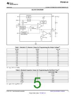
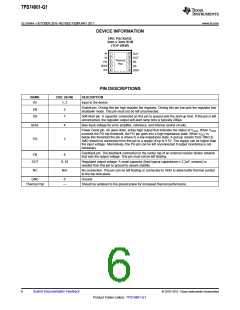
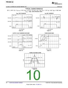
DEVICE INFORMATION
DRC PACKAGE
3mm x 3mm SON
(TOP VIEW)
IN
IN
1
2
3
4
5
10 OUT
9
8
7
6
OUT
FB
Thermal
Pad
PG
BIAS
EN
SS
GND
PIN DESCRIPTIONS
NAME
DRC (SON)
DESCRIPTION
Input to the device.
IN
1, 2
Enable pin. Driving this pin high enables the regulator. Driving this pin low puts the regulator into
shutdown mode. This pin must not be left unconnected.
EN
SS
5
7
Soft-Start pin. A capacitor connected on this pin to ground sets the start-up time. If this pin is left
unconnected, the regulator output soft-start ramp time is typically 200μs.
BIAS
4
Bias input voltage for error amplifier, reference, and internal control circuits.
Power Good pin. An open-drain, active-high output that indicates the status of VOUT. When VOUT
exceeds the PG trip threshold, the PG pin goes into a high-impedance state. When VOUT is
below this threshold the pin is driven to a low-impedance state. A pull-up resistor from 10kΩ to
1MΩ should be connected from this pin to a supply of up to 5.5V. The supply can be higher than
the input voltage. Alternatively, the PG pin can be left unconnected if output monitoring is not
necessary.
PG
3
Feedback pin. The feedback connection to the center tap of an external resistor divider network
that sets the output voltage. This pin must not be left floating.
FB
8
OUT
9, 10
Regulated output voltage. A small capacitor (total typical capacitance ≥ 2.2μF, ceramic) is
needed from this pin to ground to assure stability.
NC
N/A
No connection. This pin can be left floating or connected to GND to allow better thermal contact
to the top-side plane.
GND
6
Ground
Thermal Pad
—
Should be soldered to the ground plane for increased thermal performance.
6
Submit Documentation Feedback
© 2010–2011, Texas Instruments Incorporated
Product Folder Link(s): TPS74801-Q1

 TI [ TEXAS INSTRUMENTS ]