TPS74801-Q1
SLVSAI4A –OCTOBER 2010–REVISED FEBRUARY 2011
www.ti.com
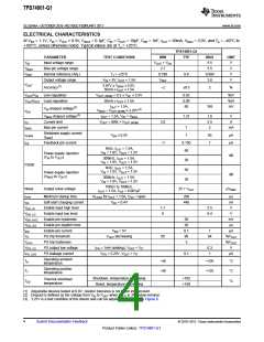
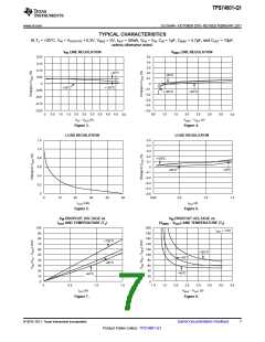
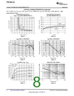
ELECTRICAL CHARACTERISTICS
At VEN = 1.1V, VIN = VOUT + 0.3V, CBIAS = 0.1μF, CIN = COUT = 10μF, CNR = 1nF, IOUT = 50mA, VBIAS = 5.0V, and TA = –40°C to
+105°C, unless otherwise noted. Typical values are at TJ = +25°C.
TPS74801-Q1
PARAMETER
TEST CONDITIONS
MIN
VOUT + VDO
2.7
TYP
MAX
5.5
UNIT
VIN
Input voltage range
Bias pin voltage range
Internal reference (Adj.)
Output voltage range
V
V
V
V
VBIAS
VREF
5.5
TJ = +25°C
0.796
0.8
0.804
3.6
VIN = 5V, IOUT = 1.5A
VREF
VOUT
2.97V ≤ VBIAS ≤ 5.5V,
50mA ≤ IOUT ≤ 1.5A
Accuracy(1)
–2
±0.5
2
%
VOUT/VIN
Line regulation
VOUT (NOM) + 0.3 ≤ VIN ≤ 5.5V
50mA ≤ IOUT ≤ 1.5A
IOUT = 1.5A,
0.03
0.09
60
%/V
%/A
mV
VOUT/IOUT Load regulation
165
VIN dropout voltage(2)
V
BIAS – VOUT (NOM) ≥ 3.25V(3)
IOUT = 1.5A, VIN = VBIAS
VOUT = 80% × VOUT (NOM)
VDO
VBIAS dropout voltage(2)
Current limit
1.31
1.6
5.5
2
V
A
ICL
2.0
IBIAS
Bias pin current
1
1
mA
Shutdown supply current
ISHDN
IFB
VEN ≤ 0.4V
50
1
μA
μA
(IGND
)
Feedback pin current
–1
0.150
60
1kHz, IOUT = 1.5A,
VIN = 1.8V, VOUT = 1.5V
Power-supply rejection
dB
(VIN to VOUT
)
300kHz, IOUT = 1.5A,
VIN = 1.8V, VOUT = 1.5V
30
50
PSRR
1kHz, IOUT = 1.5A,
VIN = 1.8V, VOUT = 1.5V
Power-supply rejection
(VBIAS to VOUT
dB
)
300kHz, IOUT = 1.5A,
VIN = 1.8V, VOUT = 1.5V
30
100Hz to 100kHz,
Noise
Output noise voltage
25 × VOUT
μVRMS
IOUT = 1.5A, CSS = 0.001μF
RLOAD for IOUT = 1.0A, CSS = open
VSS = 0.4V
tSTR
Minimum startup time
Soft-start charging current
Enable input high level
Enable input low level
Enable pin hysteresis
Enable pin deglitch time
Enable pin current
200
440
μs
nA
ISS
VEN, HI
VEN, LO
VEN, HYS
VEN, DG
IEN
1.1
0
5.5
0.4
V
V
50
20
0.1
90
3
mV
μs
VEN = 5V
1
μA
VIT
PG trip threshold
VOUT decreasing
85
94
%VOUT
%VOUT
V
VHYS
PG trip hysteresis
VPG, LO
IPG, LKG
PG output low voltage
PG leakage current
IPG = 1mA (sinking), VOUT < VIT
VPG = 5.25V, VOUT > VIT
0.3
1
0.1
μA
Operating ambient
temperature
TA
TJ
–40
–40
+105
+125
°C
°C
Operating junction
temperature
Shutdown, temperature increasing
Reset, temperature decreasing
+165
+140
Thermal shutdown
temperature
TSD
°C
(1) Adjustable devices tested at 0.8V; resistor tolerance is not taken into account.
(2) Dropout is defined as the voltage from VIN to VOUT when VOUT is 3% below nominal.
(3) 3.25V is a test condition of this device and can be adjusted by referring to Figure 8.
4
Submit Documentation Feedback
© 2010–2011, Texas Instruments Incorporated
Product Folder Link(s): TPS74801-Q1

 TI [ TEXAS INSTRUMENTS ]