TPS74801-Q1
www.ti.com
SLVSAI4A –OCTOBER 2010–REVISED FEBRUARY 2011
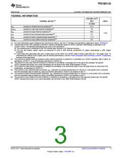
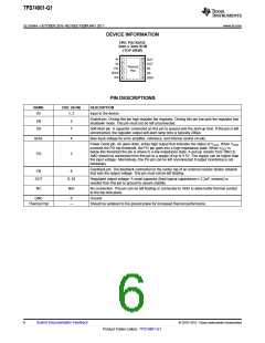
THERMAL INFORMATION
TPS74801-Q1(2)
THERMAL METRIC(1)
DRC
10 PINS
41.5
78
UNITS
θJA
Junction-to-ambient thermal resistance(3)
Junction-to-case (top) thermal resistance(4)
Junction-to-board thermal resistance(5)
Junction-to-top characterization parameter(6)
Junction-to-board characterization parameter(7)
Junction-to-case (bottom) thermal resistance(8)
θJCtop
θJB
N/A
°C/W
ψJT
0.7
ψJB
11.3
6.6
θJCbot
(1) For more information about traditional and new thermal metrics, see the IC Package Thermal Metrics application report, SPRA953A.
(2) Thermal data for the DRC package is derived by thermal simulations based on JEDEC-standard methodology as specified in the
JESD51 series. The following assumptions are used in the simulations:
(a) The exposed pad is connected to the PCB ground layer through a 3x2 thermal via array..
(b) The top and bottom copper layers are assumed to have a 20% thermal conductivity of copper representing a 20% copper
coverage.
(c) These data were generated with only a single device at the center of a JEDEC high-K (2s2p) board with 3in × 3in copper area. To
understand the effects of the copper area on thermal performance, see the Power Dissipation and Estimating Junction Temperature
sections of this data sheet.
(3) The junction-to-ambient thermal resistance under natural convection is obtained in a simulation on a JEDEC-standard, high-K board, as
specified in JESD51-7, in an environment described in JESD51-2a.
(4) The junction-to-case (top) thermal resistance is obtained by simulating a cold plate test on the top of the package. No specific
JEDEC-standard test exists, but a close description can be found in the ANSI SEMI standard G30-88.
(5) The junction-to-board thermal resistance is obtained by simulating in an environment with a ring cold plate fixture to control the PCB
temperature, as described in JESD51-8.
(6) The junction-to-top characterization parameter, ψJT, estimates the junction temperature of a device in a real system and is extracted
from the simulation data to obtain θJA using a procedure described in JESD51-2a (sections 6 and 7).
(7) The junction-to-board characterization parameter, ψJB, estimates the junction temperature of a device in a real system and is extracted
from the simulation data to obtain θJA using a procedure described in JESD51-2a (sections 6 and 7).
(8) The junction-to-case (bottom) thermal resistance is obtained by simulating a cold plate test on the exposed (power) pad. No specific
JEDEC standard test exists, but a close description can be found in the ANSI SEMI standard G30-88.
© 2010–2011, Texas Instruments Incorporated
Submit Documentation Feedback
3
Product Folder Link(s): TPS74801-Q1

 TI [ TEXAS INSTRUMENTS ]