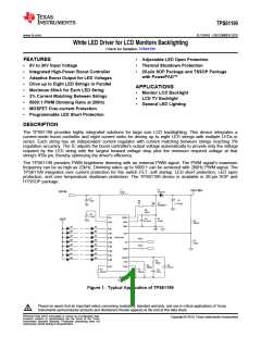
TPS61199
SLVSAN3 –DECEMBER 2010
www.ti.com
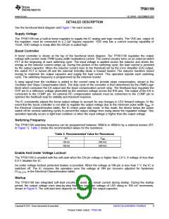
DEVICE INFORMATION
TOP VIEW
SOP - 20
(NS)
HTTSOP - 20
(PWP)
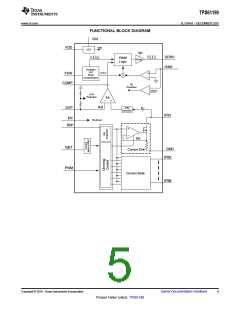
FBP
COMP
FSW
ISET
EN
1
2
3
4
5
6
7
8
9
10
OVP
VDD
VIN
20
19
18
17
16
15
14
13
12
11
FBP
COMP
FSW
ISET
EN
1
20
OVP
VDD
VIN
2
19
18
17
16
15
14
13
12
11
GDRV
ISNS
GND
IFB1
IFB2
IFB3
IFB4
3
4
GDRV
ISNS
GND
IFB1
IFB2
IFB3
IFB4
5
PWM
IFB8
IFB7
IFB6
IFB5
PWM
IFB8
IFB7
IFB6
IFB5
6
7
8
9
10
PIN ASSIGNMENTS
PIN
DESCRIPTION
NAME
VDD
EN
NO.
19
5
Internal regulator output pin. Connect a 2.2µF capacitor between this pin to GND.
Enable/disable Pin. High = IC is enabled; low = IC is disabled.
Boost switching frequency selection pin. Connect a resistor to set the frequency between 300kHz to 800
kHz
FSW
3
PWM
ISET
6
4
PWM dimming signal input pin. The frequency must be in the range of 100Hz to 22 kHz
Full-scale LED current selection pin. Connect a resistor to program LED current for each string
7, 8, 9, 10,
11
12, 13, 14
IFB1 to IFB8
Regulated current sink input pins.
Ground pin
GND
15
Loop compensation pin. Connect an RC network to make loop stable. See the relevant application
information section.
COMP
2
ISNS
GDRV
OVP
FBP
16
17
20
1
External MOSFET current sense positive input pin.
External Switch MOSFET gate driver output pin.
Over voltage protection pin. See the relevant application information section
LED short-across protection threshold program pin. See the relevant application information section
Supply input pin. This pin can be tied to a voltage different from the power stage input.
VIN
18
The PowerPAD pad must be soldered to the ground. If possible, use thermal vias to connect to top and
internal ground plane layers for ideal power dissipation.
PowerPAD in TPS61199PWP
4
Submit Documentation Feedback
Copyright © 2010, Texas Instruments Incorporated
Product Folder Link(s): TPS61199

 TI [ TEXAS INSTRUMENTS ]