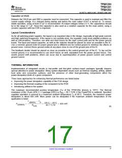
TPS61200
TPS61201
TPS61202
www.ti.com
SLVS577A–MARCH 2007–REVISED JUNE 2007
Capacitor at VAUX
Between the VAUX pin and GND a capacitor must be connected. This capacitor is used to maintain and filter the
control supply voltage. It is charged during startup and before the main output VOUT is turned on. To ensure
stable operation, using at least 0.1μF is recommended. At output voltages below 2.5 V, the capacitance should
be in the range of 1 μF. Since this capacitor is also used as a snubber capacitor for the main switch, using a
ceramic capacitor with low ESR is important.
Layout Considerations
As for all switching power supplies, the layout is an important step in the design, especially at high peak currents
and high switching frequencies. If the layout is not carefully done, the regulator could show stability problems as
well as EMI problems. Therefore, use wide and short traces for the main current path and for the power ground
tracks. The input and output capacitor, as well as the inductor should be placed as close as possible to the IC.
Use a common ground node for power ground and a different one for control ground to minimize the effects of
ground noise. Connect these ground nodes at any place close to one of the ground pins of the IC.
The feedback divider should be placed as close as possible to the control ground pin of the IC. To lay out the
control ground, it is recommended to use short traces as well, separated from the power ground traces. This
avoids ground shift problems, which can occur due to superimposition of power ground current and control
ground current.
THERMAL INFORMATION
Implementation of integrated circuits in low-profile and fine-pitch surface-mount packages typically requires
special attention to power dissipation. Many system-dependent issues such as thermal coupling, airflow, added
heat sinks and convection surfaces, and the presence of other heat-generating components affect the
power-dissipation limits of a given component.
Three basic approaches for enhancing thermal performance are listed below.
•
•
•
Improving the power dissipation capability of the PCB design
Improving the thermal coupling of the component to the PCB
Introducing airflow in the system
The maximum recommended junction temperature (TJ) of the TPS6120x devices is 125°C. The thermal
resistance of the 10-pin QFN 3 × 3 package (DRC) is RθJA = 48.7 °C/W, if the PowerPAD is soldered. Specified
regulator operation is assured to a maximum ambient temperature TA of 85°C. Therefore, the maximum power
dissipation is about 820 mW. More power can be dissipated if the maximum ambient temperature of the
application is lower.
T
* T
J(MAX)
R
A
125°C * 85°C
48.7 °CńW
P
+
+
+ 820 mW
D(MAX)
qJA
(6)
17
Submit Documentation Feedback

 TI [ TEXAS INSTRUMENTS ]