TPS61200
TPS61201
TPS61202
www.ti.com
SLVS577A–MARCH 2007–REVISED JUNE 2007
DETAILED DESCRIPTION
CONTROLLER CIRCUIT
The controlling circuit of the device is based on an average current mode topology. The average inductor current
is regulated by a fast current regulator loop which is controlled by a voltage control loop. The controller also
uses input and output voltage feedforward. Changes of input and output voltage are monitored and can
immediately change the duty cycle in the modulator to achieve a fast response to those errors. The voltage error
amplifier gets its feedback input from the FB pin. For adjustable output voltages, a resistive voltage divider must
be connected to that pin. For fixed output voltages, FB must be connected to the output voltage to directly sense
the voltage. Fixed output voltage versions use a trimmed internal resistive divider. The feedback voltage is
compared with the internal reference voltage to generate a stable and accurate output voltage.
The controller circuit also senses the average input current as well as the peak input current. Thus, the
maximum input power is controlled as well as the maximum peak current to achieve a safe and stable operation
under all possible conditions. To protect the device from overheating, an internal temperature sensor is
implemented.
Synchronous Operation
The device uses three internal N-channel MOSFETs to maintain synchronous power conversion at all possible
operating conditions. This enables the device to keep high efficiency over a wide input voltage and output power
range.
To avoid ground shift problems due to the high currents in the switches, two separate ground pins GND and
PGND are used. The reference for all control functions is the GND pin. The power switches are connected to
PGND. Both grounds must be connected on the PCB at only one point ideally close to the GND pin. Due to the
3-switch topology, the load is always disconnected from the input during shutdown of the converter.
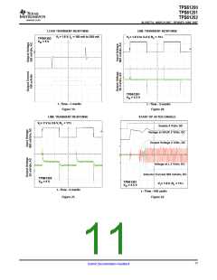
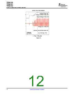
Down Regulation
A boost converter only regulates output voltages which are higher than the input voltage. This device operates
differently. For example, it is able to regulate 3 V at the output with two fresh alkaline cells at the input having a
total cell voltage of 3.2 V. Another example is powering white LEDs with a forward voltage of 3.6 V from a fully
charged Li-Ion cell with an output voltage of 4.2 V. To control these applications properly, a Down Conversion
mode is implemented.
If the input voltage reaches or exceeds the output voltage, the converter automatically changes to a Down
Conversion mode. In this mode, the control circuit changes the behavior of the two rectifying switches. While
continuing switching it sets the voltage drop across the rectifying switches as high as needed to regulate the
output voltage. This means the power losses in the converter increase. This must be taken into account for
thermal consideration.
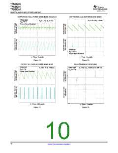
Power Save Mode
The Power Save (PS) pin can be used to select different operation modes. To enable Power Save mode the PS
pin must be set low. Power Save mode is used to improve efficiency at light load. If Power Save mode is
enabled, the converter stops operating if the average inductor current decreases below about 300 mA and the
output voltage is at or above its nominal value. If the output voltage decreases below its nominal value, the
device ramps up the output voltage again by starting operation using a programmed average inductor current
higher than required by the current load condition. Operation can last for one or several pulses. The converter
stops operating once the conditions for stopping operation are met again.
The Power Save mode can be disabled by programming high at the PS pin. In Down Conversion mode, Power
Save mode is always enabled and the device cannot be forced into fixed frequency operation at light loads. The
PS input supports standard logic thresholds.
13
Submit Documentation Feedback

 TI [ TEXAS INSTRUMENTS ]