TPS61200
TPS61201
TPS61202
www.ti.com
SLVS577A–MARCH 2007–REVISED JUNE 2007
æ
ö
V
INMIN
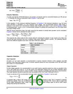
R3 = R4 x
- 1
ç
÷
ç
÷
V
UVLO
è
ø
(2)
Inductor Selection
To make sure that the TPS6120X devices can operate, an inductor must be connected between pin VIN and pin
L. To estimate the minimum inductance value Equation 3 can be used.
ms
L
= V x 0.5
IN
MIN
A
(3)
In this equation, f is the minimum switching frequency. In Equation 3, the minimum inductance, LMIN, for boost
mode operation is calculated. VIN is the maximum input voltage. The recommended inductor value range is
between 1.5 μH and 4.7 μH. The minimum inductor value should not be below 1.5 μH, even if Equation 3 yields
in something lower. Using 2.2 μH is recommended anyway for getting best performance over the whole input
and output voltage range.
With the chosen inductance value, the peak current for the inductor in steady state operation can be calculated.
Equation 4 shows how to calculate the peak current I.
V
x V
- V
IN
V
x I
OUT
(
)
IN
OUT
x f x L
OUT
OUT
0.8 x V
I
=
+
LMAX
2 x V
IN
(4)
This would be the critical value for the current rating for selecting the inductor. It also needs to be taken into
account that load transients and error conditions may cause higher inductor currents. The following inductor
series from different suppliers have been used with TPS6120x converters:
Table 1. List of Inductors
VENDOR
INDUCTOR SERIES
LPS3015
Coilcraft
LPS4012
Murata
LQH3NP
Tajo Yuden
Wurth Elektronik
NR3015
WE-TPC Typ S
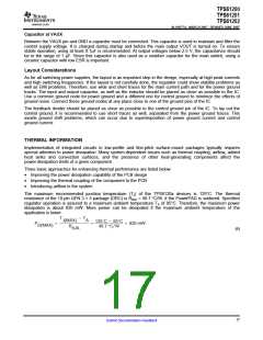
Capacitor Selection
Input Capacitor
At least a 4.7 μF input capacitor is recommended to improve transient behavior of the regulator and EMI
behavior of the total power supply circuit. A ceramic capacitor placed as close as possible to the VIN and PGND
pins of the IC is recommended.
Output Capacitor
For the output capacitor, it is recommended to use small ceramic capacitors placed as close as possible to the
VOUT and PGND pins of the IC. If, for any reason, the application requires the use of large capacitors which
can not be placed close to the IC, using a smaller ceramic capacitor in parallel to the large one is recommended.
This small capacitor should be placed as close as possible to the VOUT and PGND pins of the IC.
To get an estimate of the recommended minimum output capacitance, Equation 5 can be used.
mF
C
= 5 x L x
OUT
mH
(5)
A capacitor with a value in the range of the calculated minimum should be used. This is required to maintain
control loop stability. There are no additional requirements regarding minimum ESR. There is also no upper limit
for the output capacitance value. Larger capacitors cause lower output voltage ripple as well as lower output
voltage drop during load transients.
16
Submit Documentation Feedback

 TI [ TEXAS INSTRUMENTS ]