TPS61200
TPS61201
TPS61202
www.ti.com
SLVS577A–MARCH 2007–REVISED JUNE 2007
APPLICATION INFORMATION
DESIGN PROCEDURE
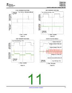
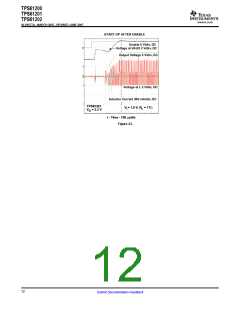
The TPS6120x DC/DC converters are intended for systems powered by a single up to triple cell Alkaline, NiCd,
NiMH battery with a typical terminal voltage between 0.7 V and 5.5 V. They can also be used in systems
powered by one-cell Li-Ion or Li-Polymer with a typical voltage between 2.5 V and 4.2 V. Additionally, any other
voltage source like solar cells or fuel cells with a typical output voltage between 0.3 V and 5.5 V can power
systems where the TPS6120x is used.
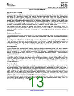
Programming the Output Voltage
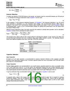
Within the TPS6120X family, there are fixed and adjustable output voltage versions available. To properly
configure the fixed output voltage devices, the FB pin is used to sense the output voltage. This means that it
must be connected directly to VOUT. At the adjustable output voltage versions, an external resistor divider is
used to adjust the output voltage. The resistor divider must be connected between VOUT, FB and GND. When
the output voltage is regulated properly, the typical value of the voltage at the FB pin is 500 mV. The maximum
recommended value for the output voltage is 5.5 V. The current through the resistive divider should be about
100 times greater than the current into the FB pin. The typical current into the FB pin is 0.01 μA, and the voltage
across the resistor between FB and GND, R2, is typically 500 mV. Based on those two values, the
recommended value for R2 should be lower than 500 kΩ, in order to set the divider current at 1 μA or higher. It
is recommended to keep the value for this resistor in the range of 200 kΩ. The value of the resistor connected
between VOUT and FB, R1, depending on the needed output voltage (VOUT), can be calculated using
Equation 1:
æ
ç
è
ö
V
OUT
R1 = R2 x
- 1
÷
V
FB
ø
(1)
If as an example, an output voltage of 3.3 V is needed, a 1-MΩ resistor should be chosen for R1 when for R2 a
180-kΩ has been selected.
L1
VIN
VIN
L
VOUT
VAUX
VOUT
C1
EN
R3
R4
R1
R2
C2
PS
C3
UVLO
FB
GND
PGND
TPS61200
Figure 24. Typical Application Circuit for Adjustable Output Voltage Option
Programming the UVLO Threshold Voltage
The UVLO input can be used to shut down the main output if the supply voltage is getting too low. The internal
reference threshold is typically 250 mV. If the supply voltage should cause the shutdown when it is dropping
below 250 mV, it can be connected directly to the UVLO pin. If the shutdown has already happen at higher
voltages, a resistor divider can be used. R3 and R4 in Figure 24 show an example of how to monitor the input
voltage of the circuit. The current through the resistive divider should be about 100 times greater than the
current into the UVLO pin. The typical current into the UVLO pin is 0.01 μA, and the voltage across R4 is equal
to the UVLO voltage threshold that is generated on-chip, which has a value of 250 mV. The recommended value
for R4 is; therefore, in the range of 250 kΩ. From this, the value of resistor R3, depending on the desired
shutdown voltage VINMIN, can be calculated using Equation 2.
15
Submit Documentation Feedback

 TI [ TEXAS INSTRUMENTS ]