TPS61020, TPS61024, TPS61025
TPS61026, TPS61027, TPS61028
TPS61029
www.ti.com
SLVS451D–SEPTEMBER 2003–REVISED FEBRUARY 2006
CAPACITOR SELECTION
Input Capacitor
At least a 10-µF input capacitor is recommended to improve transient behavior of the regulator and EMI
behavior of the total power supply circuit. A ceramic capacitor or a tantalum capacitor with a 100-nF ceramic
capacitor in parallel, placed close to the IC, is recommended.
Output Capacitor
The major parameter necessary to define the output capacitor is the maximum allowed output voltage ripple of
the converter. This ripple is determined by two parameters of the capacitor, the capacitance and the ESR. It is
possible to calculate the minimum capacitance needed for the defined ripple, supposing that the ESR is zero, by
using Equation 6:
ǒVOUT BATǓ
I
* V
OUT
C
+
min
ƒ DV V
OUT
(6)
Parameter f is the switching frequency and ∆V is the maximum allowed ripple.
With a chosen ripple voltage of 10 mV, a minimum capacitance of 24 µF is needed. The total ripple is larger due
to the ESR of the output capacitor. This additional component of the ripple can be calculated using Equation 7:
DV
+ I
R
ESR
OUT
ESR
(7)
An additional ripple of 16 mV is the result of using a tantalum capacitor with a low ESR of 80 mΩ. The total
ripple is the sum of the ripple caused by the capacitance and the ripple caused by the ESR of the capacitor. In
this example, the total ripple is 26 mV. Additional ripple is caused by load transients. This means that the output
capacitor has to completely supply the load during the charging phase of the inductor. A reasonable value of the
output capacitance depends on the speed of the load transients and the load current during the load change.
With the calculated minimum value of 24 µF and load transient considerations the recommended output
capacitance value is in a 47 to 100 µF range. For economical reasons, this is usually a tantalum capacitor.
Therefore, the control loop has been optimized for using output capacitors with an ESR of above 30 mΩ. The
minimum value for the output capacitor is 10 µF.
SMALL SIGNAL STABILITY
When using output capacitors with lower ESR, like ceramics, the adjustable voltage version is recommended.
The missing ESR can be compensated in the feedback divider. Typically a capacitor in the range of 4.7 pF in
parallel to R3 helps to obtain small signal stability with lowest ESR output capacitors. For more detailed analysis,
the small signal transfer function of the error amplifier and the regulator, which is given in Equation 8, can be
used:
4 (R3 ) R4)
R4 (1 ) i w 0.9 ms)
d
A
+
+
REG
V
FB
(8)
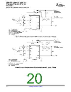
LAYOUT CONSIDERATIONS
As for all switching power supplies, the layout is an important step in the design, especially at high peak currents
and high switching frequencies. If the layout is not carefully done, the regulator could show stability problems as
well as EMI problems. Therefore, use wide and short traces for the main current path and for the power ground
tracks. The input capacitor, output capacitor, and the inductor should be placed as close as possible to the IC.
Use a common ground node for power ground and a different one for control ground to minimize the effects of
ground noise. Connect these ground nodes at any place close to one of the ground pins of the IC.
The feedback divider should be placed as close as possible to the control ground pin of the IC. To lay out the
control ground, it is recommended to use short traces as well, separated from the power ground traces. This
avoids ground shift problems, which can occur due to superimposition of power ground current and control
ground current.
17
Submit Documentation Feedback

 TI [ TEXAS INSTRUMENTS ]