TPS61020, TPS61024, TPS61025
TPS61026, TPS61027, TPS61028
TPS61029
www.ti.com
SLVS451D–SEPTEMBER 2003–REVISED FEBRUARY 2006
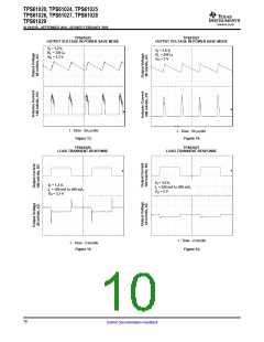
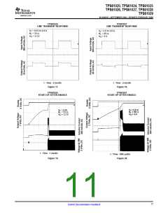
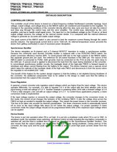
DETAILED DESCRIPTION (continued)
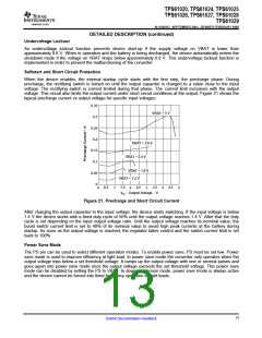
Low Battery Detector Circuit—LBI/LBO
The low-battery detector circuit is typically used to supervise the battery voltage and to generate an error flag
when the battery voltage drops below a user-set threshold voltage. The function is active only when the device
is enabled. When the device is disabled, the LBO pin is high-impedance. The switching threshold is 500 mV at
LBI. During normal operation, LBO stays at high impedance when the voltage, applied at LBI, is above the
threshold. It is active low when the voltage at LBI goes below 500 mV.
The battery voltage, at which the detection circuit switches, can be programmed with a resistive divider
connected to the LBI pin. The resistive divider scales down the battery voltage to a voltage level of 500 mV,
which is then compared to the LBI threshold voltage. The LBI pin has a built-in hysteresis of 10 mV. See the
application section for more details about the programming of the LBI threshold. If the low-battery detection
circuit is not used, the LBI pin should be connected to GND (or to VBAT) and the LBO pin can be left
unconnected. Do not let the LBI pin float.
Low-EMI Switch
The device integrates a circuit that removes the ringing that typically appears on the SW node when the
converter enters discontinuous current mode. In this case, the current through the inductor ramps to zero and
the rectifying PMOS switch is turned off to prevent a reverse current flowing from the output capacitors back to
the battery. Due to the remaining energy that is stored in parasitic components of the semiconductor and the
inductor, a ringing on the SW pin is induced. The integrated antiringing switch clamps this voltage to VBAT and
therefore dampens ringing.
14
Submit Documentation Feedback

 TI [ TEXAS INSTRUMENTS ]