TPS56528
SLVSBV3A –APRIL 2013–REVISED APRIL 2013
www.ti.com
DESIGN GUIDE
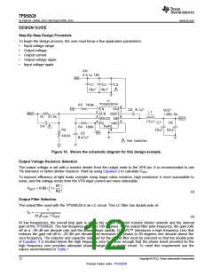
Step-By-Step Design Procedure
To begin the design process, the user must know a few application parameters:
•
•
•
•
•
Input voltage range
Output voltage
Output current
Output voltage ripple
Input voltage ripple
U1
TPS56528DDA
Figure 16. Shows the schematic diagram for this design example.
Output Voltage Resistors Selection
The output voltage is set with a resistor divider from the output node to the VFB pin. It is recommended to use
1% tolerance or better divider resistors. Start by using Equation 2 to calculate VOUT
.
To improve efficiency at light loads consider using larger value resistors, high resistance is more susceptible to
noise, and the voltage errors from the VFB input current are more noticeable.
R1
æ
ö
VOUT = 0.60´ 1+
ç
÷
R2
è
ø
(2)
Output Filter Selection
The output filter used with the TPS56528 is an LC circuit. This LC filter has double pole at:
1
F =
P
2p LOUT ´ COUT
(3)
At low frequencies, the overall loop gain is set by the output set-point resistor divider network and the internal
gain of the TPS56528. The low frequency phase is 180 degrees. At the output filter pole frequency, the gain rolls
off at a –40 dB per decade rate and the phase drops rapidly. D-CAP2™ introduces a high frequency zero that
reduces the gain roll off to –20 dB per decade and increases the phase to 90 degrees one decade above the
zero frequency. The inductor and capacitor selected for the output filter must be selected so that the double pole
of Equation 3 is located below the high frequency zero but close enough that the phase boost provided be the
high frequency zero provides adequate phase margin for a stable circuit. To meet this requirement use the
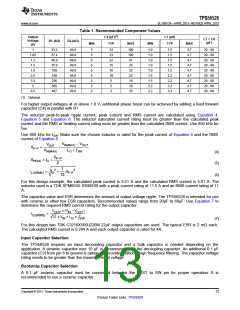
values recommended in Table 1
12
Copyright © 2013, Texas Instruments Incorporated
Product Folder Links :TPS56528

 TI [ TEXAS INSTRUMENTS ]