TPS56528
www.ti.com
SLVSBV3A –APRIL 2013–REVISED APRIL 2013
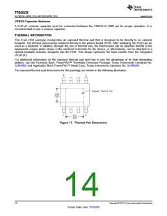
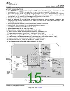
LAYOUT CONSIDERATIONS
1. The TPS56528 can supply large load currents up to 5 A, so heat dissipation may be a concern. The top side
area adjacent to the TPS56528 should be filled with ground as much as possible to dissipate heat.
2. The bottom side area directly below the IC should a dedicated ground area. It should be directed connected
to the thermal pad of the using vias as shown. The ground area should be as large as practical. Additional
internal layers can be dedicated as ground planes and connected to vias as well.
3. Keep the input switching current loop as small as possible.
4. Keep the SW node as physically small and short as possible to minimize parasitic capacitance and
inductance and to minimize radiated emissions. Kelvin connections should be brought from the output to the
feedback pin of the device.
5. Keep analog and non-switching components away from switching components.
6. Make a single point connection from the signal ground to power ground.
7. Do not allow switching current to flow under the device.
8. Keep the pattern lines for VIN and PGND broad.
9. Exposed pad of device must be connected to PGND with solder.
10. VREG5 capacitor should be placed near the device, and connected PGND.
11. Output capacitor should be connected to a broad pattern of the PGND.
12. Voltage feedback loop should be as short as possible, and preferably with ground shield.
13. Lower resistor of the voltage divider which is connected to the VFB pin should be tied to SGND.
14. Providing sufficient via is preferable for VIN, SW and PGND connection.
15. PCB pattern for VIN, SW, and PGND should be as broad as possible.
16. VIN Capacitor should be placed as near as possible to the device.
VIN
VIN
INPUT
BYPASS
CAPACITOR
VIN
HIGH FREQENCY
BYPASS
CAPACITOR
TO ENABLE
EN
VFB
VIN
VBST
SW
CONTROL
BOOST
CAPACITOR
FEEDBACK
RESISTORS
VREG5
PG
OUTPUT
VOUT
GND
INDUCTOR
POWER
GOOD
TO POWER
GOOD
PULL UP
MONITOR
EXPOSED
THERMAL PAD
AREA
BIAS
CAP
OUTPUT
FILTER
CAPACITOR
ANALOG
GROUND
TRACE
POWER GROUND
VIA to Ground Plane
Figure 18. PCB Layout
Copyright © 2013, Texas Instruments Incorporated
15
Product Folder Links :TPS56528

 TI [ TEXAS INSTRUMENTS ]