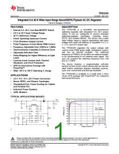
TPS55340
SLVSBD4 –MAY 2012
www.ti.com
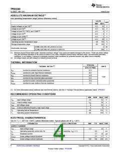
ABSOLUTE MAXIMUM RATINGS(1)
over operating temperature range (unless otherwise noted)
VALUE
UNIT
MIN
–0.3
–0.3
–0.3
–0.3
–0.3
–0.3
–40
MAX
34
34
3
Supply voltages on pin VIN(2)
Voltage on pin EN(2)
Voltage on pins FB, FREQ, and COMP(2)
Voltage on pin SS(2)
Voltage on pin SYNC(2)
Voltage on pin SW(2)
V
V
V
V
V
V
5
7
40
Operating junction temperature range
Storage temperature range
150 °C
150 °C
–65
(HBM) QSS 009-105 (JESD22-A114A)
Electrostatic discharge
2
kV
V
(CDM) QSS 009-147 (JESD22-C101B 01)
500
(1) Stresses beyond those listed under "absolute maximum ratings" may cause permanent damage to the device. These are stress ratings
only and functional operation of the device at these or any other conditions beyond those indicated under "recommended operating
conditions" is not implied. Exposure to absolute-maximum-rated conditions for extended periods may affect device reliability.
(2) All voltage values are with respect to network ground terminal
THERMAL INFORMATION
TPS55340
THERMAL METRIC(1)
UNITS
QFN (16-PINS)
θJA
Junction-to-ambient thermal resistance
43.3
38.7
14.5
0.4
θJCtop
θJB
Junction-to-case (top) thermal resistance
Junction-to-board thermal resistance
°C/W
ψJT
Junction-to-top characterization parameter
Junction-to-board characterization parameter
Junction-to-case (bottom) thermal resistance
ψJB
14.5
3.5
θJCbot
space
(1) For more information about traditional and new thermal metrics, see the IC Package Thermal Metrics application report, SPRA953.
RECOMMENDED OPERATING CONDITIONS
MIN NOM
MAX UNIT
VIN
Input voltage range
2.9
VIN
0
32
38
V
V
VOUT
VEN
VSYN
TA
Output voltage range
EN voltage range
32
V
External switching frequency logic input range
Operating free-air temperature
Operating junction temperature
0
5
V
–40
–40
125
150
°C
°C
TJ
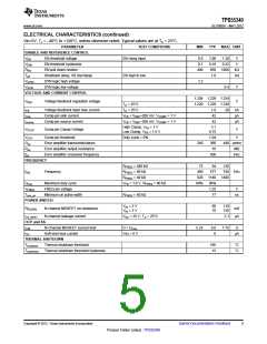
ELECTRICAL CHARACTERISTICS
Vin=5V, TJ = –40°C to +150°C, unless otherwise noted. Typical values are at TA = 25°C.
PARAMETER
TEST CONDITIONS
MIN
TYP
MAX UNIT
SUPPLY CURRENT
VIN
Input voltage range
2.9
32
V
mA
µA
V
IQ
Operating quiescent current into Vin
Shutdown current
Device non-switching, VFB = 2 V
EN = GND
0.5
2.7
ISD
10
VUVLO
Vhys
Under-voltage lockout threshold
Under-voltage lockout hysteresis
VIN falling
2.5
2.7
120
140
160 mV
4
Submit Documentation Feedback
Copyright © 2012, Texas Instruments Incorporated
Product Folder Link(s) :TPS55340

 TI [ TEXAS INSTRUMENTS ]