TPS5430
www.ti.com
SLVS632–JANUARY 2006
These devices have limited built-in ESD protection. The leads should be shorted together or the device
placed in conductive foam during storage or handling to prevent electrostatic damage to the MOS gates.
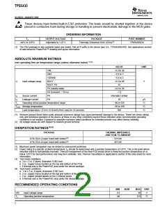
ORDERING INFORMATION
TJ
OUTPUT VOLTAGE
PACKAGE
PART NUMBER
–40°C to 125°C
Adjustable to 1.22 V
Thermally Enhanced SOIC (DDA)(1)
TPS5430DDA
(1) The DDA package is also available taped and reeled. Add an R suffix to the device type (i.e., TPS5430DDAR). See applications section
of data sheet for PowerPAD™ drawing and layout information.
ABSOLUTE MAXIMUM RATINGS
over operating free-air temperature range (unless otherwise noted)
(1)(2)
VALUE
–0.3 to 38
–0.3 to 7
–0.3 to 3
–0.3 to 48
10
UNIT
VIN
ENA
VSENSE
VI
Input voltage range
BOOT
V
BOOT-PH
PH (steady-state)
–0.6 to 38
–1.2
PH (transient < 10 ns)
IO
IO
TJ
Source current
PH
PH
Internally Limited
10
Leakage current
µA
°C
°C
°C
Operating virtual junction temperature range
–40 to 125
–65 to 150
300
TSTG Storage temperature
Lead temperature 1,6 mm (1/16-inch) from case for 10 seconds
(1) Stresses beyond those listed under absolute maximum ratings may cause permanent damage to the device. These are stress ratings
only and functional operation of the device at these or any other conditions beyond those indicated under recommended operating
conditions is not implied. Exposure to absolute-maximum-rated conditions for extended periods may affect device reliability.
(2) All voltage values are with respect to network ground terminal.
DISSIPATION RATINGS(1)(2)
PACKAGE
THERMAL IMPEDANCE
JUNCTION-TO-AMBIENT
8 Pin DDA (2-layer board with solder)(3)
8 Pin DDA (4-layer board with solder)(4)
33°C/W
26°C/W
(1) Maximum power dissipation may be limited by overcurrent protection.
(2) Power rating at a specific ambient temperature TA should be determined with a junction temperature of 125°C. This is the point where
distortion starts to substantially increase. Thermal management of the final PCB should strive to keep the junction temperature at or
below 125°C for best performance and long-term reliability. See Thermal Calculations in applications section of this data sheet for more
information.
(3) Test board conditions:
a. 3 in x 3 in, 2 layers, thickness: 0.062 inch.
b. 2 oz. copper traces located on the top and bottom of the PCB.
c. 6 thermal vias in the PowerPAD area under the device package.
(4) Test board conditions:
a. 3 in x 3 in, 4 layers, thickness: 0.062 inch.
b. 2 oz. copper traces located on the top and bottom of the PCB.
c. 2 oz. copper ground planes on the 2 internal layers.
d. 6 thermal vias in the PowerPAD area under the device package.
RECOMMENDED OPERATING CONDITIONS
MIN
5.5
NOM
MAX
36
UNIT
V
VIN
TJ
Input voltage range
Operating junction temperature
–40
125
°C
2

 TI [ TEXAS INSTRUMENTS ]