TPS54332
www.ti.com
SLVS875B –JANUARY 2009–REVISED FEBRUARY 2012
Where:
Ptot is the total device power dissipation (W).
TA is the ambient temperature (°C).
TJ is the junction temperature (°C) .
Rth is the thermal resistance of the package (°C/W).
TJMAX is maximum junction temperature (°C).
TAMAX is maximum ambient temperature (°C).
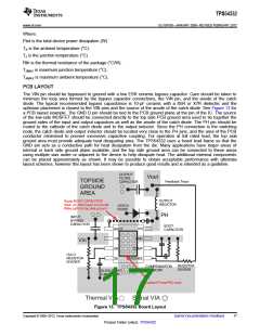
PCB LAYOUT
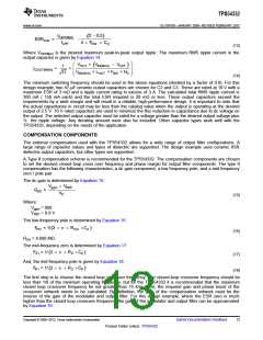
The VIN pin should be bypassed to ground with a low ESR ceramic bypass capacitor. Care should be taken to
minimize the loop area formed by the bypass capacitor connections, the VIN pin, and the anode of the catch
diode. The typical recommended bypass capacitance is 10-μF ceramic with a X5R or X7R dielectric and the
optimum placement is closest to the VIN pins and the source of the anode of the catch diode. See Figure 13 for
a PCB layout example. The GND D pin should be tied to the PCB ground plane at the pin of the IC. The source
of the low-side MOSFET should be connected directly to the top side PCB ground area used to tie together the
ground sides of the input and output capacitors as well as the anode of the catch diode. The PH pin should be
routed to the cathode of the catch diode and to the output inductor. Since the PH connection is the switching
node, the catch diode and output inductor should be located very close to the PH pins, and the area of the PCB
conductor minimized to prevent excessive capacitive coupling. For operation at full rated load, the top side
ground area must provide adequate heat dissipating area. The TPS54332 uses a fused lead frame so that the
GND pin acts as a conductive path for heat dissipation from the die. Many applications have larger areas of
internal or back side ground plane available, and the top side ground area can be connected to these areas
using multiple vias under or adjacent to the device to help dissipate heat. The additional external components
can be placed approximately as shown. It may be possible to obtain acceptable performance with alternate
layout schemes, however this layout has been shown to produce good results and is intended as a guideline.
OUTPUT
FILTER
CAPACITOR
Vout
TOPSIDE
GROUND
AREA
Feedback Trace
OUTPUT
INDUCTOR
Route BOOT CAPACITOR
trace on other layer to provide
Wide path for top side ground
CATCH
DIODE
PH
INPUT
BYPASS
CAPACITOR
BOOT
CAPACITOR
PH
BOOT
VIN
EN
GND
COMP
Vin
UVLO
RESISTOR
DIVIDER
SS
VSENSE
RESISTOR
DIVIDER
COMPENSATION
NETWORK
SLOW START
CAPACITOR
Exposed PowerPAD area
Signal VIA
Thermal VIA
Figure 13. TPS54332 Board Layout
Copyright © 2009–2012, Texas Instruments Incorporated
Submit Documentation Feedback
17
Product Folder Link(s): TPS54332

 TI [ TEXAS INSTRUMENTS ]