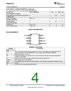
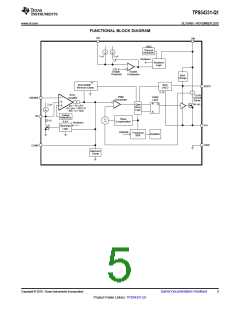
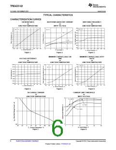
TPS54331-Q1
SLVSAB5 –NOVEMBER 2010
www.ti.com
ECO-MODETM
The TPS54331 is designed to operate in pulse skipping Eco-modeTM at light load currents to boost light load
efficiency. When the peak inductor current is lower than 160 mA typically, the COMP pin voltage falls to 0.5 V
typically and the device enters Eco-modeTM . When the device is in Eco-modeTM, the COMP pin voltage is
clamped at 0.5V internally which prevents the high side integrated MOSFET from switching. The peak inductor
current must rise above 160mA for the COMP pin voltage to rise above 0.5V and exit Eco-modeTM. Since the
integrated current comparator catches the peak inductor current only, the average load current entering
Eco-modeTM varies with the applications and external output filters.
VOLTAGE REFERENCE (Vref)
The voltage reference system produces a ±2% initial accuracy voltage reference (±3.5% over temperature) by
scaling the output of a temperature stable bandgap circuit. The typical voltage reference is designed at 0.8V.
BOOTSTRAP VOLTAGE (BOOT)
The TPS54331 has an integrated boot regulator and requires a 0.1 mF ceramic capacitor between the BOOT and
PH pin to provide the gate drive voltage for the high-side MOSFET. A ceramic capacitor with an X7R or X5R
grade dielectric is recommended because of the stable characteristics over temperature and voltage. To improve
drop out, the TPS54331 is designed to operate at 100% duty cycle as long as the BOOT to PH pin voltage is
greater than 2.1 V typically.
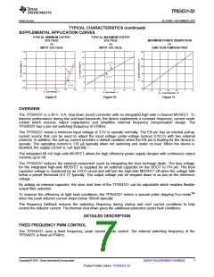
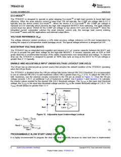
ENABLE AND ADJUSTABLE INPUT UNDER-VOLTAGE LOCKOUT (VIN UVLO)
The EN pin has an internal pull-up current source that provides the default condition of the TPS54331 operating
when the EN pin floats.
The TPS54331 is disabled when the VIN pin voltage falls below internal VIN UVLO threshold. It is recommended
to use an external VIN UVLO to add Hysteresis unless VIN is greater than (VOUT + 2 V). To adjust the VIN UVLO
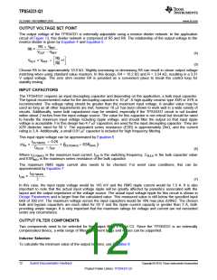
with Hysteresis, use the external circuitry connected to the EN pin as shown in Figure 12. Once the EN pin
voltage exceeds 1.25 V, an additional 3 mA of hysteresis is added. Use Equation 1 and Equation 2 to calculate
the resistor values needed for the desired VIN UVLO threshold voltages. The VSTART is the input start threshold
voltage, the VSTOP is the input stop threshold voltage and the VEN is the enable threshold voltage of 1.25 V. The
VSTOP should always be greater than 3.5 V.
TPS54331
VIN
Ren1
Ren2
1 mA
3 mA
+
-
EN
1.25 V
Figure 12. Adjustable Input Undervoltage Lockout
VSTART - VSTOP
Ren1 =
3 mA
(1)
(2)
VEN
Ren2 =
VSTART - V
EN + 1 mA
Ren1
PROGRAMMABLE SLOW START USING SS PIN
It is highly recommended to program the slow start time externally because no slow start time is implemented
8
Submit Documentation Feedback
Copyright © 2010, Texas Instruments Incorporated
Product Folder Link(s): TPS54331-Q1

 TI [ TEXAS INSTRUMENTS ]