TPS54331-Q1
www.ti.com
SLVSAB5 –NOVEMBER 2010
APPLICATION INFORMATION
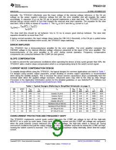
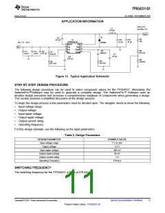
Vout 3.3 V
Iout Max 3 A
6.8 µH
0.1 μF
0Ω
47 µF
47 µF
Vin 7 V – 28 V
10.2 kΩ
3.24 kΩ
1000 pF
0.01 μF
4.7µF
4.7µF
332 kΩ
47 pF
0.01 µF
29.4 kΩ
68.1 kΩ
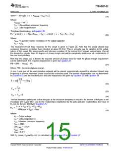
Figure 13. Typical Application Schematic
STEP BY STEP DESIGN PROCEDURE
The following design procedure can be used to select component values for the TPS54331. Alternately, the
SwitcherPro™Software may be used to generate a complete design. The SwitcherPro™ Software uses an
iterative design procedure and accesses a comprehensive database of components when generating a design.
This section presents a simplified discussion of the design process.
To begin the design process a few parameters must be decided upon. The designer needs to know the following:
•
•
•
•
•
•
Input voltage range
Output voltage
Input ripple voltage
Output ripple voltage
Output current rating
Operating frequency
For this design example, use the following as the input parameters
Table 3. Design Parameters
DESIGN PARAMETER
Input voltage range
Output voltage
EXAMPLE VALUE
7 V to 28V
3.3 V
Input ripple voltage
Output ripple voltage
Output current rating
Operating Frequency
300 mV
30 mV
3 A
570 kHz
SWITCHING FREQUENCY
The switching frequency for the TPS54331 is fixed at 570 kHz.
Copyright © 2010, Texas Instruments Incorporated
Submit Documentation Feedback
11
Product Folder Link(s): TPS54331-Q1

 TI [ TEXAS INSTRUMENTS ]