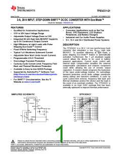
TPS54331-Q1
SLVSAB5 –NOVEMBER 2010
www.ti.com
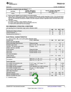
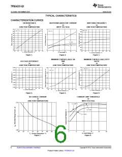
ELECTRICAL CHARACTERISTICS (continued)
TJ = –40°C to 150°C, VIN = 3.5V to 28V (unless otherwise noted)
DESCRIPTION
TEST CONDITIONS
MIN
TYP
160
5.8
MAX UNIT
PULSE SKIPPING ECO-MODE™
Pulse skipping Eco-mode™ switch current threshold
CURRENT LIMIT
mA
A
Current limit threshold
VIN = 12 V
3.5
THERMAL SHUTDOWN
Thermal Shutdown
165
°C
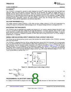
SLOW START (SS PIN)
Charge current
V(SS) = 0.4 V
V(SS) = 0.4 V
2
mA
SS to VSENSE matching
10
mV
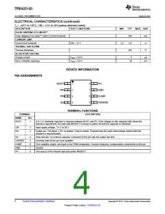
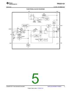
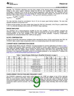
DEVICE INFORMATION
PIN ASSIGNMENTS
8
7
6
5
1
2
3
4
PH
BOOT
VIN
GND
EN
COMP
VSENSE
SS
TERMINAL FUNCTIONS
TERMINAL
DESCRIPTION
NAME
NO.
BOOT
1
A 0.1 mF bootstrap capacitor is required between BOOT and PH. If the voltage on this capacitor falls below the
minimum requirement, the high-side MOSFET is forced to switch off until the capacitor is refreshed.
VIN
EN
2
3
Input supply voltage, 3.5 V to 28 V.
Enable pin. Pull below 1.25V to disable. Float to enable. Programming the input undervoltage lockout with two
resistors is recommended.
SS
4
5
6
7
8
Slow start pin. An external capacitor connected to this pin sets the output rise time.
Inverting node of the gm error amplifier.
VSENSE
COMP
GND
PH
Error amplifier output, and input to the PWM comparator. Connect frequency compensation components to this pin.
Ground.
The source of the internal high-side power MOSFET.
4
Submit Documentation Feedback
Copyright © 2010, Texas Instruments Incorporated
Product Folder Link(s): TPS54331-Q1

 TI [ TEXAS INSTRUMENTS ]