TPS54331-Q1
www.ti.com
SLVSAB5 –NOVEMBER 2010
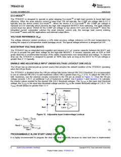
internally. The TPS54331 effectively uses the lower voltage of the internal voltage reference or the SS pin
voltage as the power supply’s reference voltage fed into the error amplifier and will regulate the output
accordingly. A capacitor (CSS) on the SS pin to ground implements a slow start time. The TPS54331 has an
internal pull-up current source of 2mA that charges the external slow start capacitor. The equation for the slow
start time (10% to 90%) is shown in Equation 3 . The Vref is 0.8 V and the ISS current is 2 mA.
CSS nF ´ V
V
( ) ref ( )
TSS ms =
( )
ISS mA
( )
(3)
The slow start time should be set between 1ms to 10 ms to ensure good start-up behavior. The slow start
capacitor should be no more than 27nF.
If during normal operation, the input voltage drops below the VIN UVLO threshold, or the EN pin is pulled below
1.25 V, or a thermal shutdown event occurs, the TPS54331 stops switching.
ERROR AMPLIFIER
The TPS54331 has a transconductance amplifier for the error amplifier. The error amplifier compares the
VSENSE voltage to the internal effective voltage reference presented at the input of the error amplifier. The
transconductance of the error amplifier is 92 mA/V during normal operation. Frequency compensation
components are connected between the COMP pin and ground.
SLOPE COMPENSATION
In order to prevent the sub-harmonic oscillations when operating the device at duty cycles greater than 50%, the
TPS54331 adds a built-in slope compensation which is a compensating ramp to the switch current signal.
CURRENT MODE COMPENSATION DESIGN
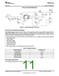
To simplify design efforts using the TPS54331, the typical designs for common applications are listed in Table 1.
For designs using ceramic output capacitors, proper derating of ceramic output capacitance is recommended
when doing the stability analysis. This is because the actual ceramic capacitance drops considerably from the
nominal value when the applied voltage increases. Advanced users may refer to the Step by Step Design
Procedure in the Application Information section for the detailed guidelines or use SwitcherPro™ Software tool
(http://focus.ti.com/docs/toolsw/folders/print/switcherpro.html).
Table 1. Typical Designs (Referring to Simplified Schematic on page 1)
VIN
(V)
VOUT
(V)
Fsw
(kHz)
Lo
(mH)
Co
RO1
(kΩ)
RO2
(kΩ)
C2
(pF)
C1
(pF)
R3
(kΩ)
12
12
12
12
12
12
12
12
5
570
570
570
570
570
570
570
570
6.8
6.8
4.7
3.3
6.8
6.8
4.7
3.3
Ceramic 33 mFx2
Ceramic 47mFx2
10
10
10
10
10
10
10
10
1.91
3.24
8.06
80.6
1.91
3.24
8.06
80.6
39
47
68
56
68
82
68
100
4700
1000
5600
5600
120
49.9
29.4
29.4
29.4
29.4
10
3.3
1.8
0.9
5
Ceramic 100 mF
Ceramic 100 mFx2
Aluminum 330 mF/160 mΩ
Aluminum 470 mF/160 mΩ
SP 100 mF/15 mΩ
3.3
1.8
0.9
220
5600
1200
29.4
49.9
SP 330 mF/12 mΩ
OVERCURRENT PROTECTION AND FREQUENCY SHIFT
The TPS54331 implements current mode control that uses the COMP pin voltage to turn off the high-side
MOSFET on a cycle by cycle basis. Every cycle the switch current and the COMP pin voltage are compared;
when the peak inductor current intersects the COMP pin voltage, the high-side switch is turned off. During
overcurrent conditions that pull the output voltage low, the error amplifier responds by driving the COMP pin high,
causing the switch current to increase. The COMP pin has a maximum clamp internally, which limit the output
current.
Copyright © 2010, Texas Instruments Incorporated
Submit Documentation Feedback
9
Product Folder Link(s): TPS54331-Q1

 TI [ TEXAS INSTRUMENTS ]