TPS51285A
TPS51285B
SLVSBX0 –APRIL 2013
www.ti.com
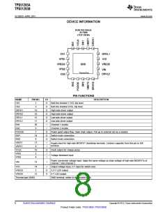
DEVICE INFORMATION
RUK PACKAGE
20 PINS
(TOP VIEW)
20
19
18
17
16
1
2
3
4
5
15
14
13
12
11
CS1
VFB1
VREG3
VFB2
CS2
DRVL1
VO1
GND
VREG5
VIN
Thermal Pad
DRVL2
6
7
8
9
10
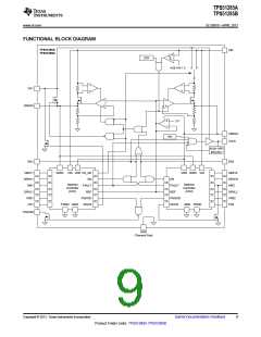
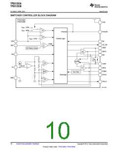
PIN FUNCTIONS
NAME
CS1
PIN NO.
I/O
O
O
O
O
O
O
I
DESCRIPTION
1
5
Sets the channel 1 OCL trip level.
Sets the channel 2OCL trip level.
High-side driver output
High-side driver output
Low-side driver output
Low-side driver output
Channel 1 enable.
CS2
DRVH1
DRVH2
DRVL1
DRVL2
EN1
16
10
15
11
20
6
EN2
I
Channel 2 enable.
PGOOD
SW1
7
O
O
O
I
Power good output flag. Open drain output. Pull up to external rail via a resistor
Switch-node connection.
18
8
SW2
Switch-node connection.
VBST1
VBST2
VCLK
VFB1
VFB2
17
9
Supply input for high-side MOSFET (bootstrap terminal). Connect capacitor from this pin to SW
terminal.
I
19
2
O
I
Clock output for charge pump.
Voltage feedback Input
4
I
Power conversion voltage input. Apply the same voltage as drain voltage of high-side MOSFETs of
channel 1 and channel 2.
VIN
12
I
VO1
14
3
I
Output voltage input, 5-V input for switch-over.
3.3-V LDO output.
VREG3
VREG5
O
O
13
5-V LDO output.
Thermal pad (GND)
GND terminal, solder to the ground plane
8
Submit Documentation Feedback
Copyright © 2013, Texas Instruments Incorporated
Product Folder Links: TPS51285A TPS51285B

 TI [ TEXAS INSTRUMENTS ]