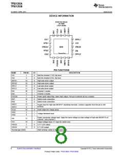
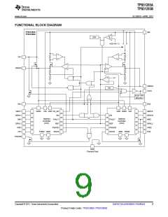
TPS51285A
TPS51285B
SLVSBX0 –APRIL 2013
www.ti.com
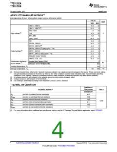
ABSOLUTE MAXIMUM RATINGS(1)
over operating free-air temperature range (unless otherwise noted)
VALUE
MIN
–0.3
–0.3
–6
UNIT
MAX
VBST1, VBST2
VBST1, VBST2(3)
SW1, SW2
32
6
26
26
6
Input voltage(2)
VIN
–0.3
–0.3
–0.3
–0.3
–6.0
–0.3
–2.5
–0.3
–2.5
–0.3
–0.3
V
EN1, EN2
VFB1, VFB2
3.6
6
VO1
DRVH1, DRVH2
32
6
DRVH1, DRVH2(3)
DRVH1, DRVH2(3) (duty cycle < 1%)
DRVL1, DRVL2
6
Output voltage(2)
6
V
DRVL1, DRVL2 (duty cycle < 1%)
PGOOD, VCLK, VREG5
VREG3, CS1, CS2
Human Boby Model (HBM)
Charged Device Model (CDM)
6
6
3.6
2
Electrostatic discharge
kV
(4)
(ESD) ratings
0.5
150
150
Junction temperature, TJ
Storage temperature, TST
°C
°C
–55
(1) Stresses beyond those listed under "absolute maximum ratings" may cause permanent damage to the device. These are stress ratings
only and functional operation of the device at these or any other conditions beyond those indicated under "recommended operating
conditions" is not implied. Exposure to absolute-maximum-rated conditions for extended periods may affect device reliability.
(2) All voltage values are with respect to the network ground terminal unless otherwise noted
(3) Voltage values are with respect to SW terminals.
(4) ESD testing is performed according to the respective JESD22 JEDEC standard.
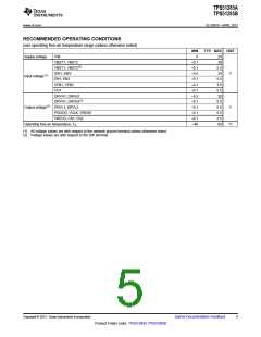
THERMAL INFORMATION
TPS51285A
TPS51285B
THERMAL METRIC(1)
UNITS
20-PIN RUK
46.2
θJA
Junction-to-ambient thermal resistance
θJCtop
θJB
Junction-to-case (top) thermal resistance
Junction-to-board thermal resistance
53.6
19.2
°C/W
ψJT
Junction-to-top characterization parameter
Junction-to-board characterization parameter
Junction-to-case (bottom) thermal resistance
0.6
ψJB
19.2
θJCbot
3.6
(1) For more information about traditional and new thermal metrics, see the IC Package Thermal Metrics application report, SPRA953.
4
Submit Documentation Feedback
Copyright © 2013, Texas Instruments Incorporated
Product Folder Links: TPS51285A TPS51285B

 TI [ TEXAS INSTRUMENTS ]