TPS386000-Q1
SBVS149 –SEPTEMBER 2010
www.ti.com
SENSE INPUT
WINDOW COMPARATOR
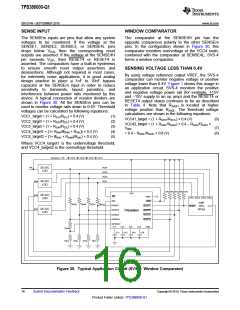
The SENSEm inputs are pins that allow any system
voltages to be monitored. If the voltage at the
SENSE1, SENSE2, SENSE3, or SENSE4L pins
drops below VITN, then the corresponding reset
outputs are asserted. If the voltage at the SENSE4H
pin exceeds VITP, then RESET4 or RESET4 is
asserted. The comparators have a built-in hysteresis
to ensure smooth reset output assertions and
deassertions. Although not required in most cases,
for extremely noise applications, it is good analog
design practice to place a 1nF to 10nF bypass
capacitor at the SENSEm input in order to reduce
sensitivity to transients, layout parasitics, and
interference between power rails monitored by this
device. A typical connection of resistor dividers are
shown in Figure 30. All the SENSEm pins can be
used to monitor voltage rails down to 0.4V. Threshold
voltages can be calculated by following equations:
The comparator at the SENSE4H pin has the
opposite comparison polarity to the other SENSEm
pins. In the configuration shown in Figure 30, this
comparator monitors overvoltage of the VCC4 node;
combined with the comparator at SENSE4L, SVS-4
forms a window comparator.
SENSING VOLTAGE LESS THAN 0.4V
By using voltage reference output VREF, the SVS-4
comparator can monitor negative voltage or positive
voltage lower than 0.4V. Figure 1 shows this usage in
an application circuit. SVS-4 monitors the positive
and negative voltage power rail (for example, +15V
and –15V supply to an op amp) and the RESET4 or
RESET4 output status continues to be as described
in Table 4. Note that RS42H is located at higher
voltage position than RS42L. The threshold voltage
calculations are shown in the following equations:
VCC1_target = (1 + RS1H/RS1L) × 0.4 (V)
VCC2_target = (1 + RS2H/RS2L) × 0.4 (V)
VCC3_target = (1 + RS3H/RS3L) × 0.4 (V)
VCC4_target1 = {1+ RS4H/®S4M + RS4L)} × 0.4 (V)
VCC4_target2 = {1+ ®S4H + RS4M)/RS4L} × 0.4 (V)
(1)
(2)
(3)
(4)
(5)
VCC41_target = (1 + RS41H/RS41L) × 0.4 (V)
(6)
VCC42_target = (1 + RS42L/RS42H) × 0.4 – RS42L/RS42H
VREF
×
(7)
(8)
= 0.4 – RS42L/RS42H × 0.8 (V)
Where VCC4_target1 is the undervoltage threshold,
and VCC4_target2 is the overvoltage threshold.
Sequence: VIN
VCC4
VCC3
VCC2
VCC1
VIN
VCC4
DC-DC
LDO
VCC3
VCC2
VCC1
EN4 DC-DC
LDO
RP5 RP4 RP3 RP2 RP1
VCC
EN3 DC-DC
LDO
MR
VREF
VCC1 VCC2 VCC3 VCC4
WDI
WDO
RESET1
RESET2
RESET3
RESET4
DSP
CPU
FPGA
RS4H
RS3H
RS2H
RS1H
SENSE1
CLK
RESET
EN2 DC-DC
LDO
SENSE2
SENSE3
SENSE4L
TPS386000
SENSE4H
CT1
CT2
CT2
CT3
CT3
CT4
CT4
GND
RS4M
RS4L
CT1
RS3L
RS2L
RS1L
Figure 30. Typical Application Circuit (SVS-4: Window Comparator)
16
Submit Documentation Feedback
Copyright © 2010, Texas Instruments Incorporated
Product Folder Link(s): TPS386000-Q1

 TI [ TEXAS INSTRUMENTS ]