TPS386000-Q1
www.ti.com
SBVS149 –SEPTEMBER 2010
RESET DELAY TIME
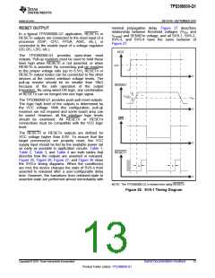
RESET1 or RESET1 is released after the
user-configured reset delay time. Note that unlike the
TPS3808 series, the TPS386000-Q1 does not
integrate an internal pull-up resistor between MR and
VCC.
Each of the SVS-n channels can be configured
independently in one of three modes. Table 6
describes the delay time settings.
Table 6. Delay Timing Selection
To control the MR function from more than one logic
signal, the logic signals can be combined by
wired-OR into the MR pin using multiple NMOS
transistors and one pull-up resistor.
CTn CONNECTION
Pull-up to VCC
Open
DELAY TIME
300ms (typ)
20 ms (typ)
Capacitor to GND
Programmable
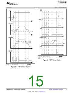
WATCHDOG TIMER
The TPS386000-Q1 provides a watchdog timer with a
dedicated watchdog error output, WDO or WDO. The
WDO or WDO output enables application board
designers to easily detect and resolve the hang-up
status of a processor. As with MR, the watchdog
timer function of the device is also tied to SVS-1.
Figure 29 shows the timing diagram of the WDT
function. Once RESET1 or RESET1 is released, the
internal watchdog timer starts its countdown. Inputting
a logic level transition at WDI resets the internal timer
count and the timer restarts the countdown. If the
TPS386000-Q1 fails to receive any WDI rising or
falling edge within the WDT period, the WDT times
out and asserts WDO or WDO. After WDO or WDO is
asserted, the device holds the status with the internal
latch circuit. To clear this timeout status, a reset
assertion of RESET1 or RESET is required. That is, a
negative pulse to MR, a SENSE1 voltage less than
VITN, or a VCC power-down is required.
To select the 300ms fixed delay time, the CTn pin
should be pulled up to VCC using a resistor from
40kΩ to 200kΩ. Note that there is a pulldown
transistor from CTn to GND that turns on every time
the device powers on to determine and confirm CTn
pin status; therefore, a direct connection of CTn to
VCC causes a large current flow. To select the 20ms
fixed delay time, the CTn pin should be left open. To
program a user-defined adjustable delay time, an
external capacitor must be connected between CTn
and GND. The adjustable delay time can be
calculated by the following equation:
CCT (nF) = [tDELAY (ms) – 0.5(ms)] × 0.242
(9)
Using this equation, a delay time can be set to
between 1.4ms to 10s. The external capacitor should
be greater than 220pF (nominal) so that the
TPS386000-Q1 can distinguish it from an open CT
pin. The reset delay time is determined by the time it
takes an on-chip, precision 300nA current source to
charge the external capacitor to 1.24V. When the
RESETn or RESETn outputs are asserted, the
corresponding capacitors are discharged. When the
condition to release RESETn or RESETn occurs, the
internal current sources are enabled and begin to
charge the external capacitors. When the CTn
To reset the processor by WDT timeout, WDO can be
combined with RESET1 by using the wired-OR with
the TPS386000-Q1 option.
For legacy applications where the watchdog timer
timeout causes RESET1 to assert, connect WDO to
MR; see Figure 30 for the connections and see
Figure 31 and Figure 32 for the timing diagram. This
legacy support configuration is available with the
TPS386000-Q1.
voltage on
a
capacitor reaches 1.24V, the
corresponding RESETn or RESETn pins are
released. Note that a low leakage type capacitor
(such as ceramic) should be used, and that stray
capacitance around this pin may cause errors in the
reset delay time.
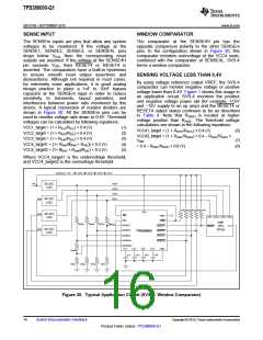
IMMUNITY TO SENSEn VOLTAGE
TRANSIENTS
The TPS386000-Q1 is relatively immune to short
negative transients on the SENSEn pin. Sensitivity to
transients depends on threshold overdrive, as shown
in the typical performance graph TPS386000-Q1
SENSEn Minimum Pulse Width vs SENSEn
Threshold Overdrive Voltage (Figure 9).
MANUAL RESET
The manual reset (MR) input allows external logic
signal from other processors, logic circuits, and/or
discrete sensors to initiate a device reset. Because
MR is connected to SVS-1, the RESET1 or RESET1
pin is intended to be connected to processor(s) as a
primary reset source. A logic low at MR causes
RESET1 or RESET1 to assert. After MR returns to a
logic high and SENSE1 is above its reset threshold,
Copyright © 2010, Texas Instruments Incorporated
Submit Documentation Feedback
17
Product Folder Link(s): TPS386000-Q1

 TI [ TEXAS INSTRUMENTS ]