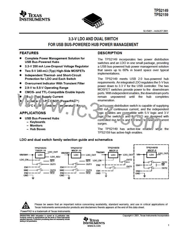
TPS2149
TPS2159
SLVS401 – AUGUST 2001
TPS2149 functional block diagram
3.3 V / 200 mA
LDO
LDO_OUT
OUT1
VIN
CS
Charge
Pump
Current
Limit
Driver
OC
EN1
Thermal
Sense
OUT2
CS
Current
Limit
Driver
EN2
Thermal
Sense
GND
Terminal Functions
TERMINAL
NO.
I/O
DESCRIPTION
NAME
TPS2149 TPS2159
EN1
EN1
EN2
EN2
GND
8
I
I
Logic level enable to transfer power to OUT1
Logic level enable to transfer power to OUT2
8
7
7
5
3
6
1
4
2
5
3
6
1
4
2
Ground
LDO_OUT
OC
O
O
O
LDO output
Overcurrent status flag for OUT1 and OUT2. Open drain output.
Switch 1 output
OUT1
OUT2
VIN
Switch 2 output
I
Input for LDO switch 1 and switch 2; device supply voltage
6
www.ti.com

 TI [ TEXAS INSTRUMENTS ]