TPS2149
TPS2159
SLVS401 – AUGUST 2001
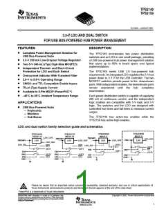
AVAILABLE OPTIONS
PACKAGED DEVICES
PACKAGE
AND PIN
COUNT
T
A
DESCRIPTION
ACTIVE LOW
ACTIVE HIGH
(SWITCH)
(SWITCH)
TPS2145IPWP
TPS2147IDGQ
Adjustable LDO with LDO enable
3.3-V fixed LDO
TSSOP-14
MSOP-10
TPS2155IPWP
TPS2157IDGQ
–40°C to 85°C
3.3-V Fixed LDO with LDO enable and LDO output
switch
MSOP-8
MSOP-8
TPS2148IDGN
TPS2149IDGN
TPS2158IDGN
TPS2159IDGN
3.3-V Fixed LDO, shared input with switches
NOTE: All options available taped and reeled. Add an R suffix (e.g. TPS2145IPWPR)
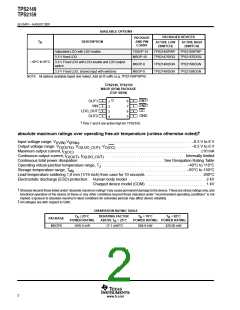
TPS2149, TPS2159
MSOP (DGN) PACKAGE
(TOP VIEW)
†
†
EN1
EN2
OC
OUT1
VIN
8
7
6
5
1
2
3
4
LDO_OUT
OUT2
GND
†
Pins 7 and 8 are active high for TPS2159.
†
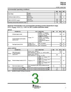
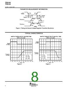
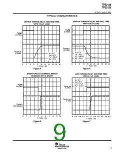
absolute maximum ratings over operating free-air temperature (unless otherwise noted)
Input voltage range: V
Output voltage range: V
Maximum output current, I
Continuous output current, I
,V
, . . . . . . . . . . . . . . . . . . . . . . . . . . . . . . . . . . . . . . . . . . . . . . . . . . . . . . . –0.3 V to 6 V
I(VIN) I(ENx)
, V
, V
. . . . . . . . . . . . . . . . . . . . . . . . . . . . . . . . . . . . . –0.3 V to 6 V
O(OUTx) O(LDO_OUT) O(OC)
. . . . . . . . . . . . . . . . . . . . . . . . . . . . . . . . . . . . . . . . . . . . . . . . . . . . . . . . . . . . . . . ±10 mA
O(OC)
O(OUT) O(LDO_OUT)
, I
. . . . . . . . . . . . . . . . . . . . . . . . . . . . . . . . . . . . . . . . . Internally limited
Continuous total power dissipation . . . . . . . . . . . . . . . . . . . . . . . . . . . . . . . . . . . . . . . . . . See Dissipation Rating Table
Operating virtual-junction temperature range, T . . . . . . . . . . . . . . . . . . . . . . . . . . . . . . . . . . . . . . . . . . –40°C to 110°C
J
Storage temperature range, T
. . . . . . . . . . . . . . . . . . . . . . . . . . . . . . . . . . . . . . . . . . . . . . . . . . . . . . . . –65°C to 150°C
stg
Lead temperature soldering 1,6 mm (1/16 inch) from case for 10 seconds . . . . . . . . . . . . . . . . . . . . . . . . . . . . 260°C
Electrostatic discharge (ESD) protection: Human body model . . . . . . . . . . . . . . . . . . . . . . . . . . . . . . . . . . . . . . . 2 kV
Charged device model (CDM) . . . . . . . . . . . . . . . . . . . . . . . . . . . . . . 1 kV
†
Stresses beyond those listed under “absolute maximum ratings” may cause permanent damage to the device. These are stress ratings only, and
functional operation of the device at these or any other conditions beyond those indicated under “recommended operating conditions” is not
implied. Exposure to absolute-maximum-rated conditions for extended periods may affect device reliability.
All voltages are with respect to GND.
‡
DISSIPATION RATING TABLE
T
≤ 25°C
DERATING FACTOR
T
= 70°C
T = 85°C
A
A
A
PACKAGE
POWER RATING
ABOVE T = 25°C
POWER RATING POWER RATING
A
MSOP8
1455.5 mW
17.1 mW/°C
684.9 mW 428.08 mW
2
www.ti.com

 TI [ TEXAS INSTRUMENTS ]