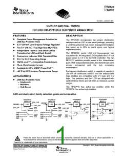
TPS2149
TPS2159
SLVS401 – AUGUST 2001
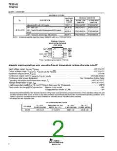
recommended operating conditions
MIN
2.9
0
MAX
5.5
UNIT
V
V
I(VIN)
Input voltage
V
5.5
I(ENx)
LDO_OUT
200
150
450
400
100
Continuous output current, I
mA
O
OUT1, OUT2
LDO_OUT
250
200
–40
Output current limit, I
mA
O(LMT)
OUT1, OUT2
Operating virtual-junction temperature range, T
°C
J
electrical characteristics over recommended operating junction-temperature range,
2.9 V ≤ V
≤ 5.5 V, T = –40°C to 100°C (unless otherwise noted)
I(VIN)
J
general
PARAMETER
TEST CONDITIONS
MIN
TYP
MAX
UNIT
V
V
V
= 5 V (inactive),
I(ENx)
Off-state supply current
= no load,
= no load
100
µA
O(LDO_OUT)
O(OUTx)
V
V
V
= 5 V (inactive),
I(ENx)
V
V
= 5 V
= 5 V,
I(VIN)
= no load,
= 0 V
O(LDO_OUT)
Forward leakage current (power
switches only)
1
µA
O(OUTx)
(measured from outputs to
ground)
I(VIN)
ENx = on (active)
ENx = off (inactive)
150
100
µA
µA
No load on OUTx,
No load on LDO_OUT
I
I
Total input current at VIN
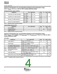
power switches
PARAMETER
TEST CONDITIONS
= 200 mA,
MIN
TYP
MAX
UNIT
I
O(LDO_OUT)
IOUT1 and IOUT2 = 150 mA, T = –40°C to 100°C
680
Static drain-source
on-state resistance,
VIN to OUTx
J
r
mΩ
DS(on)
I
= 200 mA,
O(LDO_OUT)
IOUT1 and IOUT2 = 150 mA, T = 25°C
340
J
V
V
= 5 V, V
= 5 V
= 0 V,
= 0 V,
= 0 V,
I(ENx)
I(VIN)
I(ENx)
I(ENx)
I(ENx)
10
10
V
V
= 5 V, V
= 2.9 V
I(ENx)
I(VIN)
I
I
Reverse leakage current at OUTx
Short circuit output current
V
= 5 V
µA
lkg(R)
O(OUTx)
V
V
= 5 V, V
= 0 V
I(ENx)
I(VIN)
10
OUTx connected to GND, device enabled into short
circuit
0.2
0.4
A
OS
Delay time for asserting OC flag
Delay time for deasserting OC flag
From IOUTx at 95% of current limit level to 50% OC.
From IOUTx at 95% of current limit level to 50% OC.
5.5
ms
ms
10.5
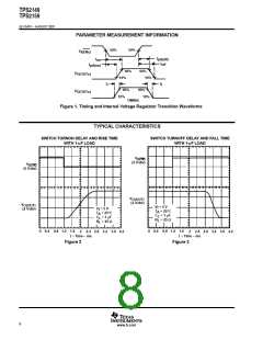
NOTE 1: Specified by design, not tested in production.
3
www.ti.com

 TI [ TEXAS INSTRUMENTS ]