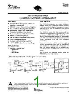
TPS2149
TPS2159
SLVS401 – AUGUST 2001
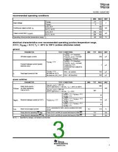
electrical characteristics over recommended operating junction-temperature range,
2.9 V ≤ V
≤ 5.5 V, T = –40°C to 100°C (unless otherwise noted)
I(VIN)
J
timing parameters, power switches
PARAMETER
TEST CONDITIONS
MIN
0.5
TYP
MAX
6
UNIT
C
C
C
C
C
C
C
C
= 100 µF
= 1 µF
L
L
L
L
L
L
L
L
t
t
t
t
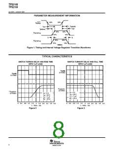
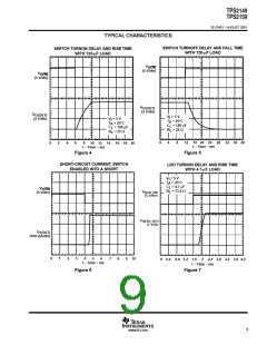
Turnon time, OUTx switch, (see Note 1)
Turnoff time, OUTx switch (see Note 1)
Rise time, OUTx switch (see Note 1)
Fall time, OUTx switch (see Note 1)
R
R
R
R
= 33 Ω
= 33 Ω
= 33 Ω
= 33 Ω
on
off
r
L
L
L
L
0.1
3
= 100 µF
= 1 µF
5.5
10
2
ms
0.05
0.5
= 100 µF
= 1 µF
5
0.1
2
= 100 µF
= 1 µF
5.5
9
f
0.05
1.2
NOTE 1. Specified by design, not tested in production.
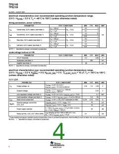
undervoltage lockout at VIN
PARAMETER
UVLO Threshold
TEST CONDITIONS
MIN
TYP
MAX
UNIT
V
2.2
2.85
Hysteresis (see Note 1)
260
mV
µs
Deglitch (see Note 1)
50
NOTE 1. Specified by design, not tested in production.
electrical characteristics over recommended operating junction-temperature range,
2.9 V ≤ V
(unless otherwise noted)
≤ 5.5 V, V
= 0 V, V
= 5 V, C
= 10 µF, T = –40°C to 100°C
I(VIN)
I(ENx)
I(LDO_EN)
L(LDO_OUT) J
3.3 V LDO
†
PARAMETER
TEST CONDITIONS
MIN
TYP
MAX
UNIT
V
= 4.25 V to 5.25 V,
I(VIN)
V
O
Output voltage, dc
Dropout voltage
3.20
3.3
3.40
V
I
= 0.5 mA to 200 mA
O(LDO_OUT)
V
= 3.2 V, I
= 150 mA,
I(VIN)
O(OUT1)
= 200 mA
0.35
V
I
O(LDO_OUT)
Line regulation voltage (see Note 1)
Load regulation voltage (see Note 1)
Short-circuit current limit
V
V
V
V
V
= 4.25 V to 5.25 V, I
= 5 mA
0.1
1%
%/V
I(VIN)
O(LDO_OUT)
= 5 mA to 200 mA
= 4.25 V, I
O(LDO_OUT)
= 4.25 V, LDO_OUT connected to GND
0.4
0.33
10
I(VIN)
I
I
0.275
0.55
A
OS
I(VIN)
= 3.3 V, V
= 5.5 V, V
= 0 V
= 0 V
µA
µA
Reverse leakage current into
LDO_OUT
O(LDO_OUT)
O(LDO_OUT)
I(IN)
I(IN)
lkg(R)
10
f = 1 kHz, C
L(LDO_OUT)
= 4.7 µF, ESR = 0.25 Ω,
= 5 mA, V = 100 mV
Power supply rejection
50
dB
ms
I
O
INp–p
V
R
ramping up from 10% to 90% in 0.1 ms,
IN
= 16 Ω, C
Ramp-up time, LDO_OUT (0% to 90%)
0.1
1
= 10 µF
L(LDO_OUT)
L
†
Pulse-testing techniques maintain junction temperature close to ambient temperature; thermal effects must be taken into account separately.
NOTES: 1. Specified by design, not tested in production.
4
www.ti.com

 TI [ TEXAS INSTRUMENTS ]