TPS2148
TPS2158
SLVS373 – AUGUST 2001
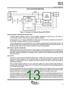
APPLICATION INFORMATION
power dissipation and junction temperature
The main source of power dissipation for the TPS2148 and TPS2158 comes from the internal voltage regulator
and the N-channel MOSFETs. Checking the power dissipation and junction temperature is always a good
designpracticeanditstartswithdeterminingther
oftheN-channelMOSFETaccordingtotheinputvoltage
(on)
DS
and operating temperature. As an initial estimate, use the highest operating ambient temperature of interest and
read r from the graphs shown in the Typical Characteristics section of this data sheet. Using this value,
(on)
DS
the power dissipation per switch can be calculated using:
2
P
r
I
D
DS(on)
(1)
(2)
Multiply this number by two to get the total power dissipation coming from the N-channel MOSFETs.
The power dissipation for the internal voltage regulator is calculated using:
P
V –V
I
D
I
O(min)
O
The total power dissipation for the device becomes:
P
P
2
P
D(total)
D(voltage regulator)
Finally, calculate the junction temperature:
D(switch)
(3)
(4)
T
P
R
T
J
D
JA
A
Where:
T = Ambient Temperature °C
A
R
= Thermal resistance °C/W, equal to inverting the derating factor found on the power
θJA
dissipation table in this datasheet.
Compare the calculated junction temperature with the initial estimate. If they do not agree within a few degrees,
repeat the calculation, using the calculated value as the new estimate. Two or three iterations are generally
sufficient to get a reasonable answer.
14
www.ti.com

 TI [ TEXAS INSTRUMENTS ]