TPS20xxC, TPS20xxC-2
SLVSAU6G –JUNE 2011–REVISED JULY 2013
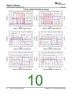
www.ti.com
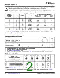
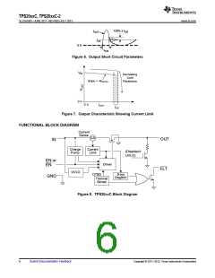
120% x I
I
OS
OUT
I
OS
0 A
t
IOS
Figure 6. Output Short Circuit Parameters
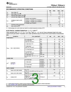
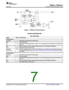
VIN
Decreasing
Load
Resistance
Slope = -RDS(ON)
0 V
0 A
IOUT
IOS
Figure 7. Output Characteristic Showing Current Limit
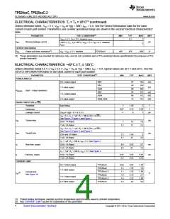
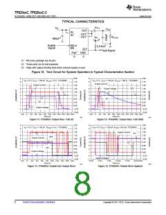
FUNCTIONAL BLOCK DIAGRAM
Current
Sense
CS
OUT
IN
Charge
Pump
Current
Limit
(Disabled+
UVLO)
EN or
EN
Driver
FLT
UVLO
9-ms
Deglitch
OTSD
Thermal
Sense
GND
Figure 8. TPS20xxC Block Diagram
6
Submit Documentation Feedback
Copyright © 2011–2013, Texas Instruments Incorporated

 TI [ TEXAS INSTRUMENTS ]