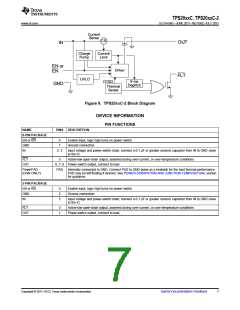
TPS20xxC, TPS20xxC-2
SLVSAU6G –JUNE 2011–REVISED JULY 2013
www.ti.com
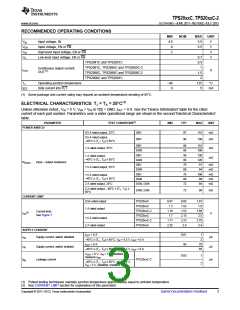
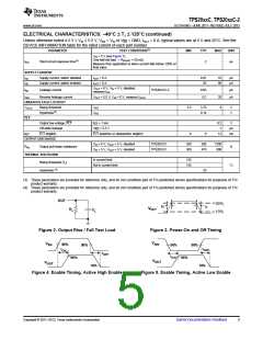
ELECTRICAL CHARACTERISTICS: TJ = TA = 25°C(1) (continued)
Unless otherwise noted:, VIN = 5 V, VEN = VIN or VEN = GND, IOUT = 0 A. See the 'Device Information' table for the rated
current of each part number. Parametrics over a wider operational range are shown in the second 'Electrical Characteristics'
table.
PARAMETER
TEST CONDITIONS(1)
MIN
TYP
MAX
UNIT
VOUT = 5 V, VIN = 0 V, measure IVOUT
0.1
1
IREV
Reverse leakage current
µA
–40°C ≤ (TJ , TA) ≤ 85°C, VOUT = 5 V, VIN = 0 V, measure
IVOUT
5
OUTPUT DISCHARGE
RPD
Output pull-down resistance(3)
VIN = VOUT = 5 V, disabled
TPS20xxC
400
470
600
Ω
(3) These parameters are provided for reference only, and do not constitute part of TI's published device specifications for purposes of TI's
product warranty.
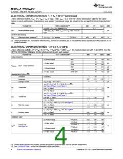
ELECTRICAL CHARACTERISTICS: –40°C ≤ TJ ≤ 125°C
Unless otherwise noted:4.5 V ≤ VIN ≤ 5.5 V, VEN = VIN or VEN = GND, IOUT = 0 A, typical values are at 5 V and 25°C. See the
DEVICE INFORMATION table for the rated current of each part number.
PARAMETER
TEST CONDITIONS(1)
MIN
TYP
MAX
UNIT
POWER SWITCH
0.5 A rated output
1 A rated output
DBV
97
96
86
76
69
72
154
154
140
121
112
112
mΩ
mΩ
DBV
DGN
RDS(ON)
Input – output resistance
DBV
mΩ
mΩ
mΩ
1.5 A rated output
2 A rated output
DGN
DGN, DGK
ENABLE INPUT (EN or EN)
Threshold
Input rising
1
0.07
–1
1.45
0.13
0
2
0.20
1
V
V
Hysteresis
Leakage current
(VEN or VEN) = 0 V or 5.5 V
µA
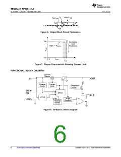
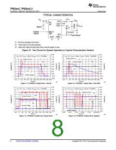
VIN = 5 V, CL = 1 µF, RL = 100 Ω, EN ↑ or EN ↓.
See Figure 2, Figure 4, and Figure 5
tON
Turnon time
Turnoff time
ms
ms
0.5A / 1A Rated
1.5A / 2A Rated
1
1.4
1.7
1.8
2.2
1.2
VIN = 5 V, CL = 1 µF, RL = 100 Ω, EN ↓ or EN ↑.
See Figure 2, Figure 4, and Figure 5
tOFF
0.5A and 1A Rated
1.3
1.7
1.65
2.1
2
1.5A / 2A Rated
2.5
CL = 1 µF, RL = 100 Ω, VIN = 5 V. See Figure 3
0.5A / 1A Rated
tR
Rise time, output
Fall time, output
0.4
0.5
0.55
0.7
0.7
1.0
ms
ms
1.5A / 2A Rated
CL = 1 µF, RL = 100 Ω, VIN = 5 V. See Figure 3
0.5A / 1A Rated
tF
0.25
0.3
0.35
0.43
0.45
0.55
1.5A / 2A Rated
CURRENT LIMIT
0.5 A rated output
1 A rated output
TPS20xxC
0.65
1.2
1.1
1.6
1.6
2.3
0.85
1.55
1.53
2.15
2.23
2.9
1.05
1.9
TPS20xxC
TPS20xxC-2
TPS20xxC
TPS20xxC-2
TPS20xxC
1.96
2.7
Current-limit,
See Figure 10
(2)
IOS
A
1.5 A rated output
2 A rated output
2.86
3.6
(1) Pulsed testing techniques maintain junction temperature approximately equal to ambient temperature
(2) See CURRENT LIMIT section for explanation of this parameter.
4
Submit Documentation Feedback
Copyright © 2011–2013, Texas Instruments Incorporated

 TI [ TEXAS INSTRUMENTS ]