TPS20xxC, TPS20xxC-2
SLVSAU6G –JUNE 2011–REVISED JULY 2013
www.ti.com
APPLICATION INFORMATION
INPUT AND OUTPUT CAPACITANCE
Input and output capacitance improves the performance of the device; the actual capacitance should be
optimized for the particular application. For all applications, a 0.1 µF or greater ceramic bypass capacitor
between IN and GND is recommended as close to the device as possible for local noise decoupling.
All protection circuits such as the TPS20xxC and TPS20xxC-2 will have the potential for input voltage overshoots
and output voltage undershoots.
Input voltage overshoots can be caused by either of two effects. The first cause is an abrupt application of input
voltage in conjunction with input power bus inductance and input capacitance when the IN terminal is high
impedance (before turn on). Theoretically, the peak voltage is 2 times the applied. The second cause is due to
the abrupt reduction of output short circuit current when the TPS20xxC and TPS20xxC-2 turns off and energy
stored in the input inductance drives the input voltage high. Input voltage droops may also occur with large load
steps and as the TPS20xxC and TPS20xxC-2 output is shorted. Applications with large input inductance (e.g.
connecting the evaluation board to the bench power-supply through long cables) may require large input
capacitance reduce the voltage overshoot from exceeding the absolute maximum voltage of the device. The fast
current-limit speed of the TPS20xxC and TPS20xxC-2 to hard output short circuits isolates the input bus from
faults. However, ceramic input capacitance in the range of 1µF to 22µF adjacent to the TPS20xxC and
TPS20xxC-2 input aids in both speeding the response time and limiting the transient seen on the input power
bus. Momentary input transients to 6.5V are permitted.
Output voltage undershoot is caused by the inductance of the output power bus just after a short has occurred
and the TPS20xxC and TPS20xxC-2 has abruptly reduced OUT current. Energy stored in the inductance will
drive the OUT voltage down and potentially negative as it discharges. Applications with large output inductance
(such as from a cable) benefit from use of a high-value output capacitor to control the voltage undershoot. When
implementing USB standard applications, a 120 µF minimum output capacitance is required. Typically a 150 µF
electrolytic capacitor is used, which is sufficient to control voltage undershoots. However, if the application does
not require 120 µF of capacitance, and there is potential to drive the output negative, a minimum of 10 µF
ceramic capacitance on the output is recommended. The voltage undershoot should be controlled to less than
1.5 V for 10 µs.
POWER DISSIPATION AND JUNCTION TEMPERATURE
It is good design practice to estimate power dissipation and maximum expected junction temperature of the
TPS20xxC and TPS20xxC-2. The system designer can control choices of package, proximity to other power
dissipating devices, and printed circuit board (PCB) design based on these calculations. These have a direct
influence on maximum junction temperature. Other factors, such as airflow and maximum ambient temperature,
are often determined by system considerations. It is important to remember that these calculations do not include
the effects of adjacent heat sources, and enhanced or restricted air flow.
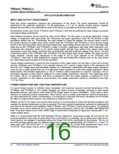
Addition of extra PCB copper area around these devices is recommended to reduce the thermal impedance and
maintain the junction temperature as low as practical. The lower junction temperatures achieved by soldering the
pad improve the efficiency and reliability of both TPS20xxC and TPS20xxC-2 parts and the system. The following
examples were used to determine the θJACustom thermal impedances noted in the THERMAL INFORMATION
table. They were based on use of the JEDEC high-k circuit board construction (2 signal and 2 plane) with 4, 1oz.
copper weight, layers.
While it is recommended that the DGN package PAD be soldered to circuit board copper fill and vias for low
thermal impedance, there may be cases where this is not desired. For example, use of routing area under the IC.
Some devices are available in packages without the Power Pad (DGK) specifically for this purpose. The θJA for
the DGN package with the pad not soldered and no extra copper, is approximately 141°C/W for 0.5 - A and 1- A
rated parts, and 139°C/W for the 1.5 - A and 2- A rated parts. The θJA for the DGK mounted per Figure 45 is
110.3C/W. These values may be used in Equation 1 to determine the maximum junction temperature.
16
Submit Documentation Feedback
Copyright © 2011–2013, Texas Instruments Incorporated

 TI [ TEXAS INSTRUMENTS ]