TPS20xxC, TPS20xxC-2
SLVSAU6G –JUNE 2011–REVISED JULY 2013
www.ti.com
DETAILED DESCRIPTION
The TPS20xxC and TPS20xxC-2 are current-limited, power-distribution switches providing between 0.5 A and 2
A of continuous load current in 5 V circuits. These parts use N-channel MOSFETs for low resistance, maintaining
voltage regulation to the load. They are designed for applications where short circuits or heavy capacitive loads
will be encountered. Device features include enable, reverse blocking when disabled, output discharge pulldown,
overcurrent protection, over-temperature protection, and deglitched fault reporting.
UVLO
The undervoltage lockout (UVLO) circuit disables the power switch until the input voltage reaches the UVLO turn-
on threshold. Built-in hysteresis prevents unwanted on/off cycling due to input voltage drop from large current
surges. FLT is high impedance when the TPS20xxC and TPS20xxC-2 are in UVLO.
ENABLE
The logic enable input (EN, or EN), controls the power switch, bias for the charge pump, driver, and other
circuits. The supply current is reduced to less than 1 µA when the TPS20xxC and TPS20xxC-2 are disabled.
Disabling the TPS20xxC and TPS20xxC-2 will immediately clear an active FLT indication. The enable input is
compatible with both TTL and CMOS logic levels.
The turnon and turnoff times (tON, tOFF) are composed of a delay and a rise or fall time (tR, tF). The delay times
are internally controlled. The rise time is controlled by both the TPS20xxC and TPS20xxC-2 and the external
loading (especially capacitance). TPS20xxC fall time is controlled by the loading (R and C), and the output
discharge (RPD). TPS20xxC-2 does not have the output discharge (RPD), fall time is controlled by the loading (R
and C). An output load consisting of only a resistor will experience a fall time set by the TPS20xxC and
TPS20xxC-2. An output load with parallel R and C elements will experience a fall time determined by the (R × C)
time constant if it is longer than the TPS20xxC and TPS20xxC-2’s tF.
The enable should not be left open, and may be tied to VIN or GND depending on the device.
INTERNAL CHARGE PUMP
The device incorporates an internal charge pump and gate drive circuitry necessary to drive the N-channel
MOSFET. The charge pump supplies power to the gate driver circuit and provides the necessary voltage to pull
the gate of the MOSFET above the source. The driver incorporates circuitry that controls the rise and fall times of
the output voltage to limit large current and voltage surges on the input supply, and provides built-in soft-start
functionality. The MOSFET power switch will block current from OUT to IN when turned off by the UVLO or
disabled.
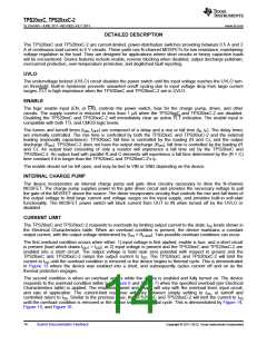
CURRENT LIMIT
The TPS20xxC and TPS20xxC-2 responds to overloads by limiting output current to the static IOS levels shown in
the Electrical Characteristics table. When an overload condition is present, the device maintains a constant
output current, with the output voltage determined by (IOS × RLOAD). Two possible overload conditions can occur.
The first overload condition occurs when either: 1) input voltage is first applied, enable is true, and a short circuit
is present (load which draws IOUT > IOS), or 2) input voltage is present and the TPS20xxC and TPS20xxC-2 are
enabled into a short circuit. The output voltage is held near zero potential with respect to ground and the
TPS20xxC and TPS20xxC-2 ramps the output current to IOS. The TPS20xxC and TPS20xxC-2 will limit the
current to IOS until the overload condition is removed or the device begins to thermal cycle. This is demonstrated
in Figure 13 where the device was enabled into a short, and subsequently cycles current off and on as the
thermal protection engages.
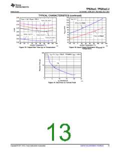
The second condition is when an overload occurs while the device is enabled and fully turned on. The device
responds to the overload condition within tIOS (Figure 6 and Figure 7) when the specified overload (per Electrical
Characteristics table) is applied. The response speed and shape will vary with the overload level, input circuit,
and rate of application. The current-limit response will vary between simply settling to IOS, or turnoff and
controlled return to IOS. Similar to the previous case, the TPS20xxC and TPS20xxC-2 will limit the current to IOS
until the overload condition is removed or the device begins to thermal cycle. This is demonstrated by Figure 14,
Figure 15, and Figure 16.
14
Submit Documentation Feedback
Copyright © 2011–2013, Texas Instruments Incorporated

 TI [ TEXAS INSTRUMENTS ]