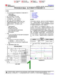
TPS1HC30-Q1
ZHCSP75A –JULY 2022 –REVISED DECEMBER 2022
www.ti.com.cn
(2) 器件将在更广的工作电压范围工作,但某些时序参数值可能不适用。有关使用的电压,请参阅相应章节。此外,有关更多说明,请参见
节9.3。
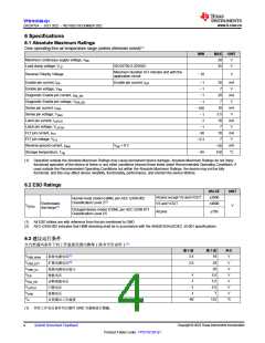
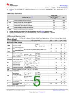
6.4 Thermal Information
TPS1HC30-Q1
THERMAL METRIC(1) (2)
PWP (HTSSOP)
UNIT
14 PINS
44.2
33.8
19.2
1.4
RθJA
Junction-to-ambient thermal resistance
Junction-to-case (top) thermal resistance
Junction-to-board thermal resistance
°C/W
°C/W
°C/W
°C/W
°C/W
°C/W
RθJC(top)
RθJB
Junction-to-top characterization parameter
Junction-to-board characterization parameter
Junction-to-case (bottom) thermal resistance
ψJT
19.2
5.0
ψJB
RθJC(bot)
(1) For more information about traditional and new thermal metrics, see the SPRA953 application report.
(2) The thermal parameters are based on a 4-layer PCB according to the JESD51-5 and JESD51-7 standards.
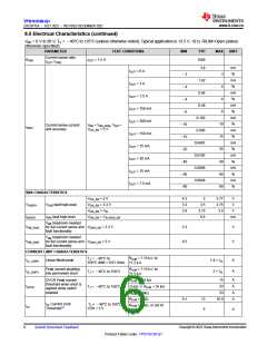
6.5 Electrical Characteristics
VBB = 6 V to 28 V, TA = –40°C to 125°C (unless otherwise noted); Typical application is 13.5 V, 10 Ω, RILIM=Open (unless
otherwise specified)
PARAMETER
TEST CONDITIONS
MIN
TYP
MAX
UNIT
INPUT VOLTAGE AND CURRENT
TJ=25°C
35
33
43
45
V
V
VClamp
VDS clamp voltage
TJ = –40°C to 150°C
VBB undervoltage lockout
rising
VUVLOR
VUVLOF
3.0
2.4
3.5
2.6
4.0
3.0
V
V
Measured with respect to the GND pin of the device
VBB undervoltage lockout
falling
TJ = 25°C
0.3
2.5
9
µA
µA
µA
µA
µA
Standby current (total
device leakage including
MOSFET channel)
VBB ≤18 V, VEN
VDIA_EN = 0 V, VOUT = 0 V
=
ISB
TJ = 85°C
TJ = 125°C
TJ = 25°C
TJ = 85°C
0.01
0.3
2.5
VBB ≤18 V, VEN
VDIA_EN = 0 V, VOUT = 0 V
=
IOUT(standby) Output leakage current
Current consumption in
diagnostic mode
VBB ≤18 V, ISNS = 0 mA
VEN = 0 V, VDIA_EN = 5 V, VOUT = 0V
IDIA
1.3
1.6
3
3
mA
mA
Quiescent current
channel enabled
VBB ≤28 V
VEN = VDIA_EN = 5 V, IOUTx = 0 A
IQ
ILNOM
tSTBY
Continuous load current Channel enabled, TAMB = 85°C
Standby mode delay time VENx = VDIA_EN = 0 V to standby
4.5
20
A
ms
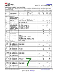
RON CHARACTERISTICS
TJ = 25°C
TJ = 150°C
TJ = 25°C
TJ = 150°C
TJ = 25°C
TJ = 150°C
30
mΩ
mΩ
mΩ
mΩ
mΩ
mΩ
6 V ≤VBB ≤28 V,
IOUT= 1 A
On-resistance
(Includes MOSFET
channel and metallization
on die)
57
57
75
RON
3 V ≤VBB ≤6 V,
IOUT =1 A
30
On-resistance during
reverse polarity
RON(REV)
-18 V ≤VBB ≤-6 V
57
1
Source-to-drain body
diode voltage
VF
0.3
0.7
V
VEN = 0 V IOUT = –1 A
CURRENT SENSE CHARACTERISTICS
Copyright © 2023 Texas Instruments Incorporated
Submit Document Feedback
5
Product Folder Links: TPS1HC30-Q1

 TI [ TEXAS INSTRUMENTS ]