TPS1HC30-Q1
ZHCSP75A –JULY 2022 –REVISED DECEMBER 2022
www.ti.com.cn
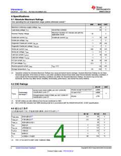
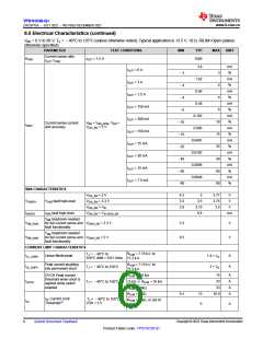
6 Specifications
6.1 Absolute Maximum Ratings
Over operating free-air temperature range (unless otherwise noted)(1)
MIN
MAX
UNIT
V
Maximum continuous supply voltage, VBB
28
35
Load dump voltage, VLD
Reverse Polarity Voltage
ISO16750-2:2010(E)
V
Maximum duration of 3 minutes and with the
application circuit
V
–18
Enable pin current, IEN
Enable pin current, IEN
20
7
mA
V
–1
–1
Enable pin voltage, VEN
Diagnostic Enable pin current, IDIA_EN
Diagnostic Enable pin voltage, VDIA_EN
Sense pin current, ISNS
20
7
mA
V
–1
–1
10
5.5
10
7
mA
V
–100
–1
Sense pin voltage, VSNS
Latch pin current, ILATCH
Latch pin voltage, VLATCH
FLT pin current, IFLT
-1
mA
V
–1
-30
10
7
mA
V
FLT pin voltage, VFLT
–0.3
Reverse ground current, IGND
Storage temperature, Tstg
VBB < 0 V
mA
°C
–50
150
–65
(1) Operation outside the Absolute Maximum Ratings may cause permanent device damage. Absolute Maximum Ratings do not imply
functional operation of the device at these or any other conditions beyond those listed under Recommended Operating Conditions. If
used outside the Recommended Operating Conditions but within the Absolute Maximum Ratings, the device may not be fully
functional, and this may affect device reliability, functionality, performance, and shorten the device lifetime.
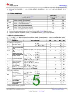
6.2 ESD Ratings
VALUE
±2000
±4000
UNIT
All pins except VS and VOUT
VS and VOUT
Human-body model (HBM), per AEC Q100-002
Classification Level 2(2)
Electrostatic
discharge(1)
V(ESD)
V
Charged-device model (CDM), per AEC Q100-011
Classification Level C5
All pins
±750
(1) All ESD strikes are with reference from the pin mentioned to GND
(2) AEC-Q100-002 indicates that HBM stressing shall be in accordance with the ANSI/ESDA/JEDEC JS-001 specifications.
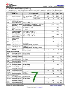
6.3 建议运行条件
在自然通风条件下的工作温度范围内测得(除非另有说明)(1)
最小值
最大值
单位
标称电源电压(1)
扩展电源电压(2)
短路电源电压能力
使能电压
VVBB_NOM
VVBB_EXT
VVBB_SC
VEN
3.5
18
V
V
2.6
28
28
V
-1
-1
5.5
5.5
5.5
7
V
VDIA_EN
VLATCH
VSNS
V
诊断使能电压
闩锁电压
-1
V
-1
V
检测电压
TA
-40
125
°C
自然通风工作温度
(1) 所有工作电压条件均以器件GND 为基准进行测量。
Copyright © 2023 Texas Instruments Incorporated
4
Submit Document Feedback
Product Folder Links: TPS1HC30-Q1

 TI [ TEXAS INSTRUMENTS ]