TPS1H100-Q1
www.ti.com.cn
ZHCSDD8D –OCTOBER 2014–REVISED DECEMBER 2019
9 Power Supply Recommendations
The device is qualified for both automotive and industrial applications. The normal power supply connection is a
12-V automotive system or 24-V industrial system. The supply voltage should be within the range specified in the
Recommended Operating Conditions.
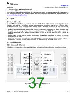
10 Layout
10.1 Layout Guidelines
To prevent thermal shutdown, TJ must be less than 150°C. If the output current is very high, the power
dissipation may be large. The HTSSOP package has good thermal impedance. However, the PCB layout is very
important. Good PCB design can optimize heat transfer, which is absolutely essential for the long-term reliability
of the device.
•
Maximize the copper coverage on the PCB to increase the thermal conductivity of the board. The major heat-
flow path from the package to the ambient is through the copper on the PCB. Maximum copper is extremely
important when there are not any heat sinks attached to the PCB on the other side of the board opposite the
package.
•
•
Add as many thermal vias as possible directly under the package ground pad to optimize the thermal
conductivity of the board.
All thermal vias should either be plated shut or plugged and capped on both sides of the board to prevent
solder voids. To ensure reliability and performance, the solder coverage should be at least 85%.
10.2 Layout Example
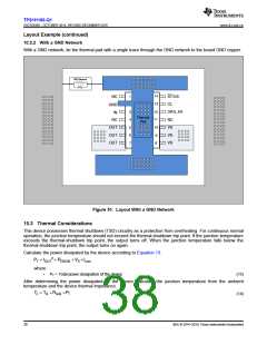
10.2.1 Without a GND Network
Without a GND network, tie the thermal pad directly to the board GND copper for better thermal performance.
14
NC
ST/CS
CL
1
2
3
4
5
6
7
13
GND
IN
DIAG_EN
12
11
Thermal
Pad
NC
NC
VS
VS
VS
10
OUT
OUT
OUT
9
8
Figure 50. Layout Without a GND Network
Copyright © 2014–2019, Texas Instruments Incorporated
37

 TI [ TEXAS INSTRUMENTS ]