TPS1H100-Q1
ZHCSDD8D –OCTOBER 2014–REVISED DECEMBER 2019
www.ti.com.cn
However, an inductive load is not acceptable to avoid an abnormal status when switching off.
•
Type 3 (resistor and diode in parallel (recommended)): A peak negative spike may occur when the
inductive load is switching off, which may damage the HSD or the diode. So, TI recommends a resistor in
parallel with the diode when driving an inductive load. The recommended selection are 1-kΩ resistor in
parallel with an IF > 100-mA diode. If multiple high-side switches are used, the resistor and diode can be
shared among devices.
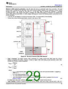
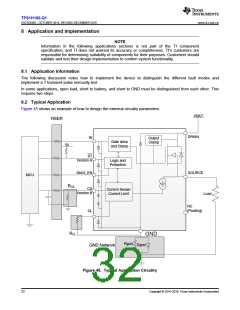
7.3.4.10 Protection for MCU I/Os
In many conditions, such as the negative ISO pulse, or the loss of battery with an inductive load, a negative
potential on the device GND pin may damage the MCU I/O pins [more likely, the internal circuitry connected to
the pins]. Therefore, the serial resistors between MCU and HSD are required.
Also, for proper protection against loss of GND, TI recommends 4.7 kΩ when using 3.3-V MCU I/Os; 10 kΩ is for
5-V applications.
VBAT
DRAIN
IN
Output
Clamp
Gate drive
and Clamp
5V
STATUS
Version A
Logic and
Protection
DIAG_EN
SOURCE
MCU
CS
Version B
Current Sense/
Current Limit
Load
NC
(Floating)
CURRENT
LIMIT
GND
Rgnd
Dgnd
Figure 43. MCU IO Protections
7.3.5 Diagnostic Enable Function
The diagnostic enable pin, DIAG_EN, offers multiplexing of the microcontroller diagnostic input for current sense
or digital status, by sharing the same sense resistor and ADC line or I/O port among multiple devices.
30
Copyright © 2014–2019, Texas Instruments Incorporated

 TI [ TEXAS INSTRUMENTS ]