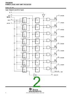
TPIC6B595
POWER LOGIC 8-BIT SHIFT REGISTER
SLIS032 – JULY 1995
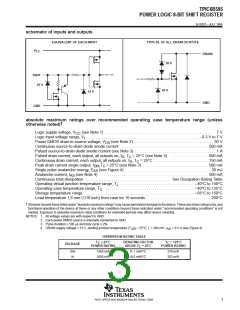
recommended operating conditions
MIN
MAX
UNIT
V
Logic supply voltage, V
CC
4.5
5.5
High-level input voltage, V
IH
0.85 V
V
CC
Low-level input voltage, V
0.15 V
V
IL
Pulsed drain output current, T = 25°C, V
CC
= 5 V (see Notes 3 and 5)
CC
–500
20
500
mA
ns
ns
ns
°C
C
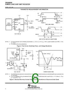
Setup time, SER IN high before SRCK↑, t (see Figure 2)
su
Hold time, SER IN high after SRCK↑, t (see Figure 2)
20
h
Pulse duration, t (see Figure 2)
40
w
Operating case temperature, T
–40
125
C
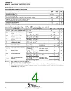
electrical characteristics, V
= 5 V, T = 25°C (unless otherwise noted)
CC
C
PARAMETER
TEST CONDITIONS
MIN
TYP
MAX
UNIT
V
V
Drain-to-source breakdown voltage
I
I
= 1 mA
50
V
(BR)DSX
D
Source-to-drain diode forward
voltage
= 100 mA
0.85
1
V
V
SD
F
I
I
I
I
= –20 µA, V
= 4.5 V
= 4.5 V
= 4.5 V
= 4.5 V
4.4
4
4.49
4.2
High-level output voltage,
SER OUT
OH
OH
OL
OL
CC
CC
CC
CC
V
OH
OL
= –4 mA,
= 20 µA,
= 4 mA,
V
V
V
0.005
0.3
0.1
0.5
1
Low-level output voltage,
SER OUT
V
V
I
I
High-level input current
Low-level input current
V
= 5.5 V, V = V
CC
µA
µA
IH
CC
CC
I
V
= 5.5 V, V = 0
I
–1
IL
All outputs off
All outputs on
20
100
300
I
Logic supply current
V
CC
= 5.5 V
µA
CC
150
f
= 5 MHzC, = 30 pF,
L
SRCK
I
Logic supply current at frequency
Nominal current
0.4
90
5
mA
mA
CC(FRQ)
N
All outputs off,
See Figures 2 and 6
See Notes 5, 6, and 7
V
= 0.5 V,
DS(on)
= I ,
I
I
N
T = 85°C
C
D
V
= 40 V,
V
V
V
= 5.5 V
0.1
0.15
4.2
5
8
DS
DS
CC
CC
CC
I
Off-state drain current
µA
DSX
V
= 40 V,
= 5.5 V,
= 4.5 V
T = 125°C
C
I
I
= 100 mA,
5.7
D
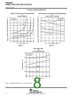
Static drain-source on-state
resistance
= 100 mA,
= 4.5 V
T
C
= 125°C, See Notes 5 and 6
D
r
Ω
6.8
5.5
9.5
8
DS(on)
V
and Figures 7 and 8
CC
= 350 mA,
I
D
V
CC
= 4.5 V
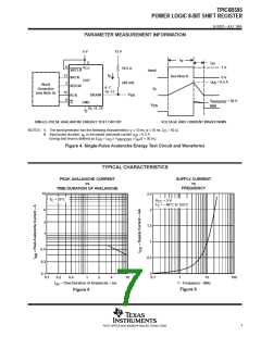
NOTES: 3. Pulse duration ≤ 100 µs and duty cycle ≤ 2%.
5. Technique should limit T – T to 10°C maximum.
J
C
6. These parameters are measured with voltage-sensing contacts separate from the current-carrying contacts.
7. Nominal current is defined for a consistent comparison between devices from different sources. It is the current that produces a
voltage drop of 0.5 V at T = 85°C.
C
4
POST OFFICE BOX 655303 • DALLAS, TEXAS 75265

 TI [ TEXAS INSTRUMENTS ]