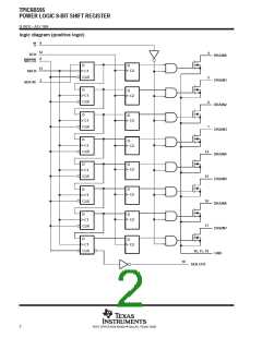
TPIC6B595
POWER LOGIC 8-BIT SHIFT REGISTER
SLIS032 – JULY 1995
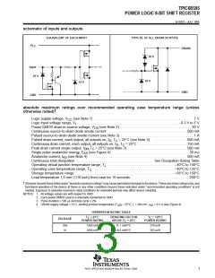
schematic of inputs and outputs
EQUIVALENT OF EACH INPUT
TYPICAL OF ALL DRAIN OUTPUTS
V
CC
DRAIN
50 V
Input
25 V
20 V
12 V
GND
GND
absolute maximum ratings over recommended operating case temperature range (unless
†
otherwise noted)
Logic supply voltage, V
(see Note 1) . . . . . . . . . . . . . . . . . . . . . . . . . . . . . . . . . . . . . . . . . . . . . . . . . . . . . . . 7 V
CC
Logic input voltage range, V . . . . . . . . . . . . . . . . . . . . . . . . . . . . . . . . . . . . . . . . . . . . . . . . . . . . . . . . –0.3 V to 7 V
Power DMOS drain-to-source voltage, V
I
(see Note 2) . . . . . . . . . . . . . . . . . . . . . . . . . . . . . . . . . . . . . . . . 50 V
DS
Continuous source-to-drain diode anode current . . . . . . . . . . . . . . . . . . . . . . . . . . . . . . . . . . . . . . . . . . . . 500 mA
Pulsed source-to-drain diode anode current (see Note 3) . . . . . . . . . . . . . . . . . . . . . . . . . . . . . . . . . . . . . . . . . 1 A
Pulsed drain current, each output, all outputs on, I , T = 25°C (see Note 3) . . . . . . . . . . . . . . . . . . . 500 mA
D
C
Continuous drain current, each output, all outputs on, I , T = 25°C . . . . . . . . . . . . . . . . . . . . . . . . . . . 150 mA
D
C
Peak drain current single output, I ,T = 25°C (see Note 3) . . . . . . . . . . . . . . . . . . . . . . . . . . . . . . . . . 500 mA
DM
C
Single-pulse avalanche energy, E (see Figure 4) . . . . . . . . . . . . . . . . . . . . . . . . . . . . . . . . . . . . . . . . . . . 30 mJ
AS
Avalanche current, I (see Note 4) . . . . . . . . . . . . . . . . . . . . . . . . . . . . . . . . . . . . . . . . . . . . . . . . . . . . . . 500 mA
AS
Continuous total dissipation . . . . . . . . . . . . . . . . . . . . . . . . . . . . . . . . . . . . . . . . . . . See Dissipation Rating Table
Operating virtual junction temperature range, T . . . . . . . . . . . . . . . . . . . . . . . . . . . . . . . . . . . . . –40°C to 150°C
J
Operating case temperature range, T
. . . . . . . . . . . . . . . . . . . . . . . . . . . . . . . . . . . . . . . . . . . . . –40°C to 125°C
C
Storage temperature range . . . . . . . . . . . . . . . . . . . . . . . . . . . . . . . . . . . . . . . . . . . . . . . . . . . . . . . . –65°C to 150°C
Lead temperature 1,6 mm (1/16 inch) from case for 10 seconds . . . . . . . . . . . . . . . . . . . . . . . . . . . . . . . 260°C
†
Stresses beyond those listed under “absolute maximum ratings” may cause permanent damage to the device. These are stress ratings only, and
functional operation of the device at these or any other conditions beyond those indicated under “recommended operating conditions” is not
implied. Exposure to absolute-maximum-rated conditions for extended periods may affect device reliability.
NOTES: 1. All voltage values are with respect to GND.
2. Each power DMOS source is internally connected to GND.
3. Pulse duration ≤ 100 µs and duty cycle ≤ 2%.
4. DRAIN supply voltage = 15 V, starting junction temperature (T ) = 25°C, L = 200 mH, I
= 0.5 A (see Figure 4).
AS
JS
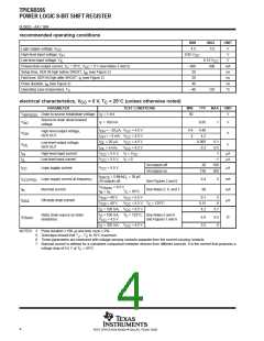
DISSIPATION RATING TABLE
T
≤ 25°C
DERATING FACTOR
T = 125°C
C
POWER RATING
C
PACKAGE
POWER RATING
ABOVE T = 25°C
C
DW
N
1389 mW
11.1 mW/°C
10.5 mW/°C
278 mW
1050 mW
263 mW
3
POST OFFICE BOX 655303 • DALLAS, TEXAS 75265

 TI [ TEXAS INSTRUMENTS ]