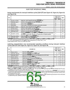
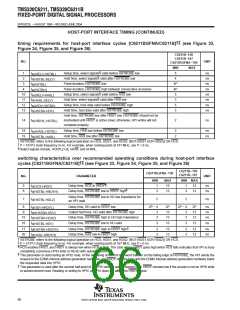
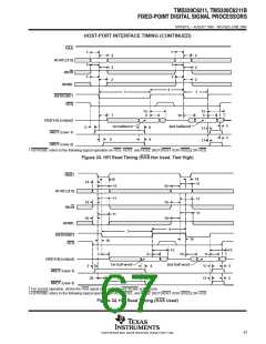
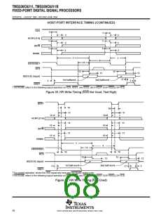
ꢀ ꢁꢂ ꢃ ꢄ ꢅ ꢆꢇ ꢄ ꢈꢈ ꢉ ꢀ ꢁꢂ ꢃ ꢄꢅ ꢆꢇ ꢄꢈꢈꢊ
ꢋ ꢌꢍ ꢎꢏꢐꢑꢒ ꢌ ꢓꢀ ꢏꢌ ꢔꢌ ꢀꢕꢖ ꢂꢌ ꢔ ꢓꢕꢖ ꢑꢗ ꢒ ꢆꢎ ꢂ ꢂꢒ ꢗ ꢂ
SPRS073L − AUGUST 1998 − REVISED JUNE 2004
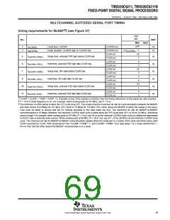
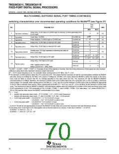
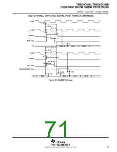
MULTICHANNEL BUFFERED SERIAL PORT TIMING
†‡
timing requirements for McBSP (see Figure 37)
−150
−167
NO.
UNIT
MIN
MAX
§
2
3
t
t
Cycle time, CLKR/X
CLKR/X ext
CLKR/X ext
CLKR int
CLKR ext
CLKR int
CLKR ext
CLKR int
CLKR ext
CLKR int
CLKR ext
CLKX int
CLKX ext
CLKX int
CLKX ext
2P
ns
ns
c(CKRX)
Pulse duration, CLKR/X high or CLKR/X low
0.5t
c(CKRX)
− 1
20
1
w(CKRX)
5
6
t
t
t
t
t
t
Setup time, external FSR high before CLKR low
Hold time, external FSR high after CLKR low
Setup time, DR valid before CLKR low
ns
ns
ns
ns
ns
ns
su(FRH-CKRL)
h(CKRL-FRH)
su(DRV-CKRL)
h(CKRL-DRV)
su(FXH-CKXL)
h(CKXL-FXH)
6
3
22
3
7
3
8
Hold time, DR valid after CLKR low
4
23
1
10
11
Setup time, external FSX high before CLKX low
Hold time, external FSX high after CLKX low
6
3
†
‡
§
CLKRP = CLKXP = FSRP = FSXP = 0. If polarity of any of the signals is inverted, then the timing references of that signal are also inverted.
P = 1/CPU clock frequency in ns. For example, when running parts at 167 MHz, use P = 6 ns.
The minimum CLKR/X period is twice the CPU cycle time (2P). This means that the maximum bit rate for communications between the McBSP
and other device is 83 Mbps for 167 MHz CPU clock or 75 Mbps for 150 MHz CPU clock; where the McBSP is either the master or the slave.
Care must be taken to ensure that the AC timings specified in this data sheet are met. The maximum bit rate for McBSP-to-McBSP
communications is 33 Mbps; therefore, the minimum CLKR/X clock cycle is either twice the CPU cycle time (2P), or 30 ns (33 MHz), whichever
value is larger. For example, when running parts at 167 MHz (P = 6 ns), use 30 ns as the minimum CLKR/X clock cycle (by setting the appropriate
CLKGDV ratio or external clock source). When running parts at 60 MHz (P = 16.67 ns), use 2P = 33 ns (30 MHz) as the minimum CLKR/X clock
cycle. The maximum bit rate for McBSP-to-McBSP communications applies when the serial port is a master of the clock and frame syncs (with
CLKR connected to CLKX, FSR connected to FSX, CLKXM = FSXM = 1, and CLKRM = FSRM = 0) in data delay 1 or 2 mode (R/XDATDLY =
01b or 10b) and the other device the McBSP communicates to is a slave.
69
POST OFFICE BOX 1443 • HOUSTON, TEXAS 77251−1443

 TI [ TEXAS INSTRUMENTS ]