ꢀ ꢁꢂ ꢃ ꢄ ꢅ ꢆꢇ ꢄ ꢈꢈ ꢉ ꢀ ꢁꢂ ꢃ ꢄꢅ ꢆꢇ ꢄꢈꢈꢊ
ꢋ ꢌꢍ ꢎꢏꢐꢑꢒ ꢌ ꢓꢀ ꢏꢌ ꢔꢌ ꢀꢕꢖ ꢂꢌ ꢔ ꢓꢕꢖ ꢑꢗ ꢒ ꢆꢎ ꢂ ꢂꢒ ꢗ ꢂ
SPRS073L − AUGUST 1998 − REVISED JUNE 2005
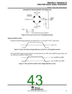
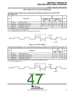
PARAMETER MEASUREMENT INFORMATION
I
OL
Tester Pin
Electronics
Output
Under
Test
50 Ω
V
comm
C
T
I
OH
Where:
I
I
V
=
=
=
=
2 mA
2 mA
0.8 V
OL
OH
comm
T
C
10−15-pF typical load-circuit capacitance
Figure 9. Test Load Circuit for AC Timing Measurements
signal transition levels
All input and output timing parameters are referenced to 1.5 V for both “0” and “1” logic levels.
V
ref
= 1.5 V
Figure 10. Input and Output Voltage Reference Levels for ac Timing Measurements
All rise and fall transition timing parameters are referenced to V MAX and V MIN for input clocks, and
IL
IH
V
MAX and V
MIN for output clocks.
OL
OH
V
ref
= V MIN (or V
IH OH
MIN)
V
ref
= V MAX (or V
IL OL
MAX)
Figure 11. Rise and Fall Transition Time Voltage Reference Levels
43
POST OFFICE BOX 1443 • HOUSTON, TEXAS 77251−1443

 TI [ TEXAS INSTRUMENTS ]