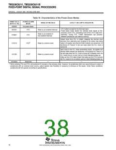
ꢀ ꢁ ꢂ ꢃ ꢄꢅ ꢆ ꢇ ꢄꢈꢈ ꢉ ꢀꢁ ꢂꢃ ꢄ ꢅ ꢆꢇ ꢄ ꢈꢈ ꢊ
ꢋ ꢌ ꢍꢎꢏ ꢐꢑ ꢒꢌ ꢓ ꢀ ꢏ ꢌ ꢔꢌ ꢀꢕꢖ ꢂ ꢌ ꢔꢓ ꢕꢖ ꢑ ꢗꢒ ꢆꢎꢂ ꢂꢒ ꢗꢂ
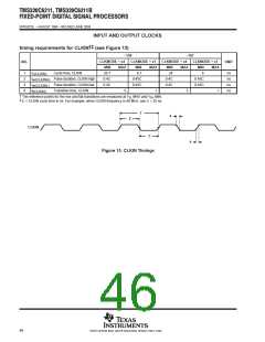
SPRS073L − AUGUST 1998 − REVISED JUNE 2005
†
absolute maximum ratings over operating case temperature range (unless otherwise noted)
Supply voltage range, CV
Supply voltage range, DV
(see Note 1) . . . . . . . . . . . . . . . . . . . . . . . . . . . . . . . . . . . . . . . . . . . − 0.3 V to 2.3 V
(see Note 1) . . . . . . . . . . . . . . . . . . . . . . . . . . . . . . . . . . . . . . . . . . . . . −0.3 V to 4 V
DD
DD
Input voltage range . . . . . . . . . . . . . . . . . . . . . . . . . . . . . . . . . . . . . . . . . . . . . . . . . . . . . . . . . . . . . . . . . −0.3 V to 4 V
Output voltage range . . . . . . . . . . . . . . . . . . . . . . . . . . . . . . . . . . . . . . . . . . . . . . . . . . . . . . . . . . . . . . . −0.3 V to 4 V
Operating case temperature ranges, T :(default) . . . . . . . . . . . . . . . . . . . . . . . . . . . . . . . . . . . . 0_C to 90_C
C
(A version) [C6211BGFNA only] . . . . . . . . . . . . . . −40_C to105_C
Storage temperature range, T . . . . . . . . . . . . . . . . . . . . . . . . . . . . . . . . . . . . . . . . . . . . . . . −65_C to 150_C
stg
†
Stresses beyond those listed under “absolute maximum ratings” may cause permanent damage to the device. These are stress ratings only, and
functional operation of the device at these or any other conditions beyond those indicated under “recommended operating conditions” is not
implied. Exposure to absolute-maximum-rated conditions for extended periods may affect device reliability.
NOTE 1: All voltage values are with respect to V
SS
.
recommended operating conditions
MIN NOM
MAX UNIT
CV
DV
Supply voltage, Core
Supply voltage, I/O
Supply ground
1.71
3.14
0
1.8
3.3
0
1.89
3.46
0
V
V
DD
DD
V
V
V
V
SS
High-level input voltage
Low-level input voltage
2
V
IH
IL
0.8
−4
−8
4
V
All signals except CLKOUT1, CLKOUT2, and ECLKOUT
CLKOUT1, CLKOUT2, and ECLKOUT
All signals except CLKOUT1, CLKOUT2, and ECLKOUT
CLKOUT1, CLKOUT2, and ECLKOUT
Default
mA
mA
mA
mA
_C
_C
I
I
High-level output current
Low-level output current
Operating case temperature
OH
OL
8
0
90
105
T
C
A version (C6211BGFNA only)
−40
electrical characteristics over recommended ranges of supply voltage and operating case
temperature (unless otherwise noted)
‡
PARAMETER
High-level output voltage
Low-level output voltage
Input current
TEST CONDITIONS
MIN
TYP
MAX
UNIT
V
V
V
DV
DV
= MIN,
= MIN,
I
= MAX
= MAX
2.4
OH
DD
DD
OH
OL
I
0.4
150
10
V
OL
I
I
V = V
I SS
to DV
DD
uA
uA
mA
mA
mA
mA
mA
mA
pF
I
Off-state output current
V
= DV
or 0 V
= NOM, CPU clock = 150 MHz
= NOM, CPU clock = 150 MHz
= NOM, CPU clock = 150 MHz
OZ
O DD
C6211, CV
DD
270
270
220
220
60
Supply current, CPU + CPU memory
I
I
I
DD2V
§
access
C6211B, CV
DD
C6211, CV
DD
§
Supply current, peripherals
DD2V
DD3V
C6211B, CV
= NOM, CPU clock = 150 MHz
= NOM, CPU clock = 150 MHz
DD
C6211, DV
DD
§
Supply current, I/O pins
C6211B, DV
DD
= NOM, CPU clock = 150 MHz
60
C
C
Input capacitance
Output capacitance
7
7
i
pF
o
‡
§
For test conditions shown as MIN, MAX, or NOM, use the appropriate value specified in the recommended operating conditions table.
Measured with average activity (50% high/50% low power). For more details on CPU, peripheral, and I/O activity, refer to the TMS320C62x/C67x
Power Consumption Summary application report (literature number SPRA486).
42
POST OFFICE BOX 1443 • HOUSTON, TEXAS 77251−1443

 TI [ TEXAS INSTRUMENTS ]