ꢀ ꢁ ꢂ ꢃ ꢄꢅ ꢆ ꢇ ꢄꢈꢈ ꢉ ꢀꢁ ꢂꢃ ꢄ ꢅ ꢆꢇ ꢄ ꢈꢈ ꢊ
ꢋ ꢌ ꢍꢎꢏ ꢐꢑ ꢒꢌ ꢓ ꢀ ꢏ ꢌ ꢔꢌ ꢀꢕꢖ ꢂ ꢌ ꢔꢓ ꢕꢖ ꢑ ꢗꢒ ꢆꢎꢂ ꢂꢒ ꢗꢂ
SPRS073L − AUGUST 1998 − REVISED JUNE 2005
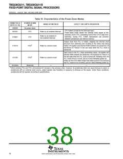
Table 19. Characteristics of the Power-Down Modes
PRWD FIELD
(BITS 15−10)
POWER-DOWN
WAKE-UP METHOD
—
EFFECT ON CHIP’S OPERATION
MODE
000000
001001
No power-down
—
CPU halted (except for the interrupt logic)
PD1
Wake by an enabled interrupt
Power-down mode blocks the internal clock inputs at the
boundary of the CPU, preventing most of the CPU’s logic from
switching. During PD1, EDMA transactions can proceed
between peripherals and internal memory.
Wake by an enabled or
non-enabled interrupt
010001
011010
PD1
Output clock from PLL is halted, stopping the internal clock
structure from switching and resulting in the entire chip being
halted. All register and internal RAM contents are preserved. All
functional I/O “freeze” in the last state when the PLL clock is
turned off.
†
PD2
Wake by a device reset
Input clock to the PLL stops generating clocks. All register and
internal RAM contents are preserved. All functional I/O “freeze” in
the last state when the PLL clock is turned off. Following reset, the
PLL needs time to re-lock, just as it does following power-up.
Wake-up from PD3 takes longer than wake-up from PD2 because
the PLL needs to be re-locked, just as it does following power-up.
†
PD3
011100
Wake by a device reset
All others
Reserved
—
—
†
When entering PD2 and PD3, all functional I/O remains in the previous state. However, for peripherals which are asynchronous in nature or
peripherals with an external clock source, output signals may transition in response to stimulus on the inputs. Under these conditions,
peripherals will not operate according to specifications.
38
POST OFFICE BOX 1443 • HOUSTON, TEXAS 77251−1443

 TI [ TEXAS INSTRUMENTS ]