ꢀ ꢁꢂ ꢃ ꢄ ꢅ ꢆꢇ ꢄ ꢈꢈ ꢉ ꢀ ꢁꢂ ꢃ ꢄꢅ ꢆꢇ ꢄꢈꢈꢊ
ꢋ ꢌꢍ ꢎꢏꢐꢑꢒ ꢌ ꢓꢀ ꢏꢌ ꢔꢌ ꢀꢕꢖ ꢂꢌ ꢔ ꢓꢕꢖ ꢑꢗ ꢒ ꢆꢎ ꢂ ꢂꢒ ꢗ ꢂ
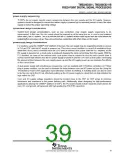
SPRS073L − AUGUST 1998 − REVISED JUNE 2005
clock PLL (continued)
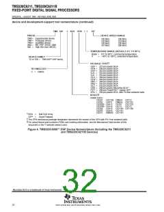
3.3V
PLLV
Internal to
PLL
C6211/C6211B
CLKMODE0
CLKIN
PLLMULT
CLKIN
PLLCLK
1
0
LOOP FILTER
CPU
CLOCK
NOTES: A. For a system with ONLY PLL x1 (bypass) mode, short the PLLF terminal to the PLLG terminal.
B. The 3.3-V supply for the EMI filter must be from the same 3.3-V power plane supplying the I/O voltage, DV
.
DD
Figure 6. External PLL Circuitry for x1 (Bypass) Mode Only
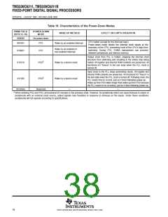
Table 18. C6211/C6211B PLL Component Selection
CPU CLOCK
FREQUENCY
(CLKOUT1)
CLKIN
RANGE
(MHz)
CLKOUT2
RANGE
(MHz)
TYPICAL
R1 [ 1%]
C1 [ 10%]
(nF)
C2 [ 10%]
CLKMODE
LOCK TIME
(Ω)
(pF)
†
(µs)
RANGE (MHz)
x4
16.3−41.6
65−167
32.5−83
60.4
27
560
75
†
Under some operating conditions, the maximum PLL lock time may vary as much as 150% from the specified typical value. For example, if the
typical lock time is specified as 100 µs, the maximum value may be as long as 250 µs.
35
POST OFFICE BOX 1443 • HOUSTON, TEXAS 77251−1443

 TI [ TEXAS INSTRUMENTS ]