ꢀ ꢁꢂ ꢃ ꢄ ꢅ ꢆꢇ ꢄ ꢈꢈ ꢉ ꢀ ꢁꢂ ꢃ ꢄꢅ ꢆꢇ ꢄꢈꢈꢊ
ꢋ ꢌꢍ ꢎꢏꢐꢑꢒ ꢌ ꢓꢀ ꢏꢌ ꢔꢌ ꢀꢕꢖ ꢂꢌ ꢔ ꢓꢕꢖ ꢑꢗ ꢒ ꢆꢎ ꢂ ꢂꢒ ꢗ ꢂ
SPRS073L − AUGUST 1998 − REVISED JUNE 2005
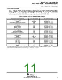
memory map summary
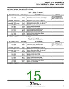
Table 2 shows the memory map address ranges of the C6211/C6211B devices. Internal memory is always
located at address 0 and can be used as both program and data memory. The C6211/C6211B configuration
registers for the common peripherals are located at the same hex address ranges. The external memory
address ranges in the C6211/C6211B devices begin at the address location 0x8000 0000.
Table 2. TMS320C6211/C6211B Memory Map Summary
MEMORY BLOCK DESCRIPTION
Internal RAM (L2)
BLOCK SIZE (BYTES)
HEX ADDRESS RANGE
0000 0000 – 0000 FFFF
0001 0000 – 017F FFFF
0180 0000 – 0183 FFFF
0184 0000 – 0187 FFFF
0188 0000 – 018B FFFF
018C 0000 – 018F FFFF
0190 0000 – 0193 FFFF
0194 0000 – 0197 FFFF
0198 0000 – 019B FFFF
019C 0000 – 019F FFFF
01A0 0000 – 01A3 FFFF
01A4 0000 – 01FF FFFF
0200 0000 – 0200 0033
0200 0034 – 2FFF FFFF
3000 0000 – 3FFF FFFF
4000 0000 – 7FFF FFFF
8000 0000 – 8FFF FFFF
9000 0000 – 9FFF FFFF
A000 0000 – AFFF FFFF
B000 0000 – BFFF FFFF
C000 0000 – FFFF FFFF
64K
24M – 64K
256K
Reserved
External Memory Interface (EMIF) Registers
L2 Registers
256K
HPI Registers
256K
McBSP 0 Registers
McBSP 1 Registers
Timer 0 Registers
256K
256K
256K
Timer 1 Registers
256K
Interrupt Selector Registers
EDMA RAM and EDMA Registers
Reserved
256K
256K
6M – 256K
52
QDMA Registers
Reserved
736M – 52
256M
1G
McBSP 0/1 Data
Reserved
†
†
†
†
EMIF CE0
EMIF CE1
EMIF CE2
EMIF CE3
256M
256M
256M
256M
1G
Reserved
†
The number of EMIF address pins (EA[21:2]) limits the maximum addressable memory (SDRAM) to 128MB per CE space. To get 256MB of
addressable memory, additional general-purpose output pin or external logic is required.
11
POST OFFICE BOX 1443 • HOUSTON, TEXAS 77251−1443

 TI [ TEXAS INSTRUMENTS ]