TMS320F28027, TMS320F28027-Q1, TMS320F28027F, TMS320F28027F-Q1, TMS320F28026
TMS320F28026-Q1, TMS320F28026F, TMS320F28026F-Q1, TMS320F28023
TMS320F28023-Q1, TMS320F28022, TMS320F28021, TMS320F28020, TMS320F280200
ZHCSA13P –NOVEMBER 2008 –REVISED FEBRUARY 2021
www.ti.com.cn
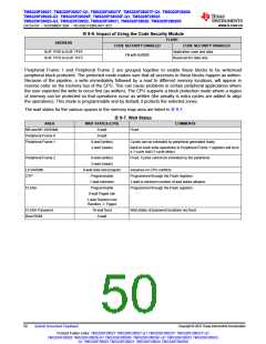
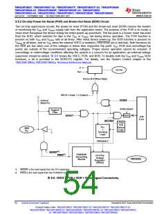
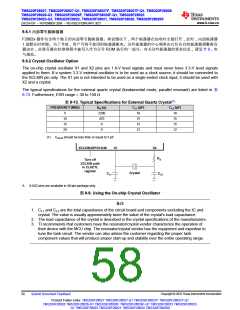
9.5.2 On-chip Power-On Reset (POR) and Brown-Out Reset (BOR) Circuit
Two on-chip supervisory circuits, the power-on reset (POR) and the brown-out reset (BOR) remove the burden
of monitoring the VDD and VDDIO supply rails from the application board. The purpose of the POR is to create a
clean reset throughout the device during the entire power-up procedure. The trip point is a looser, lower trip point
than the BOR, which watches for dips in the VDD or VDDIO rail during device operation. The POR function is
present on both VDD and VDDIO rails at all times. After initial device power-up, the BOR function is present on
VDDIO at all times, and on VDD when the internal VREG is enabled ( VREGENZ pin is tied low). Both functions tie
the XRS pin low when one of the voltages is below their respective trip point. VDD BOR and overvoltage trip
points are outside of the recommended operating voltages. Proper device operation cannot be ensured. If
overvoltage or undervoltage conditions affecting the system is a concern for an application, an external voltage
supervisor should be added. 图 9-6 shows the VREG, POR, and BOR. To disable both the VDD and VDDIO BOR
functions, a bit is provided in the BORCFG register. For details, see the System Control chapter in the
TMS320F2802x,TMS320F2802xx Technical Reference Manual.
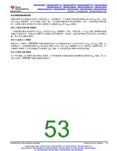
In
I/O Pin
Out
(Force Hi-Z When High)
DIR (0 = Input, 1 = Output)
Internal
Weak PU
SYSRS
SYSCLKOUT
Deglitch
Filter
Sync
RS
WDRST
C28
Core
MCLKRS
PLL
JTAG
TCK
Detect
Logic
XRS
Pin
+
Clocking
Logic
VREGHALT
WDRST(A)
PBRS(B)
POR/BOR
Generating
Module
On-Chip
Voltage
Regulator
(VREG)
VREGENZ
A. WDRST is the reset signal from the CPU watchdog.
B. PBRS is the reset signal from the POR/BOR module.
图9-6. VREG + POR + BOR + Reset Signal Connectivity
Copyright © 2022 Texas Instruments Incorporated
54
Submit Document Feedback
Product Folder Links: TMS320F28027 TMS320F28027-Q1 TMS320F28027F TMS320F28027F-Q1
TMS320F28026 TMS320F28026-Q1 TMS320F28026F TMS320F28026F-Q1 TMS320F28023 TMS320F28023-
Q1 TMS320F28022 TMS320F28021 TMS320F28020 TMS320F280200

 TI [ TEXAS INSTRUMENTS ]