TMS320F28027, TMS320F28027-Q1, TMS320F28027F, TMS320F28027F-Q1, TMS320F28026
TMS320F28026-Q1, TMS320F28026F, TMS320F28026F-Q1, TMS320F28023
TMS320F28023-Q1, TMS320F28022, TMS320F28021, TMS320F28020, TMS320F280200
ZHCSA13P –NOVEMBER 2008 –REVISED FEBRUARY 2021
www.ti.com.cn
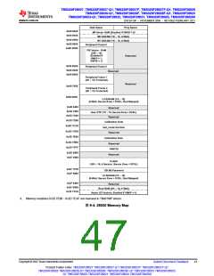
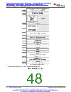
9.3 Register Maps
The devices contain three peripheral register spaces. The spaces are categorized as follows:
Peripheral Frame 0:
Peripheral Frame 1:
Peripheral Frame 2:
These are peripherals that are mapped directly to the CPU memory bus. See 表9-8.
These are peripherals that are mapped to the 32-bit peripheral bus. See 表9-9.
These are peripherals that are mapped to the 16-bit peripheral bus. See 表9-10.
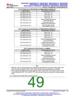
表9-8. Peripheral Frame 0 Registers
NAME(1)
Device Emulation Registers
System Power Control Registers
FLASH Registers(3)
ADDRESS RANGE
0x00 0880 to 0x00 0984
0x00 0985 to 0x00 0987
0x00 0A80 to 0x00 0ADF
0x00 0AE0 to 0x00 0AEF
0x00 0B00 to 0x00 0B0F
0x00 0C00 to 0x00 0C3F
0x00 0CE0 to 0x00 0CFF
0x00 0D00 to 0x00 0DFF
SIZE (×16)
EALLOW PROTECTED(2)
261
3
Yes
Yes
Yes
Yes
No
96
16
16
64
32
256
Code Security Module Registers
ADC registers (0 wait read only)
CPU–TIMER0/1/2 Registers
PIE Registers
No
No
PIE Vector Table
No
(1) Registers in Frame 0 support 16-bit and 32-bit accesses.
(2) If registers are EALLOW protected, then writes cannot be performed until the EALLOW instruction is executed. The EDIS instruction
disables writes to prevent stray code or pointers from corrupting register contents.
(3) The Flash Registers are also protected by the Code Security Module (CSM).
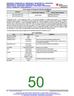
表9-9. Peripheral Frame 1 Registers
NAME
Comparator 1 registers
ADDRESS RANGE
0x00 6400 to 0x00 641F
0x00 6420 to 0x00 643F
0x00 6800 to 0x00 683F
0x00 6840 to 0x00 687F
0x00 6880 to 0x00 68BF
0x00 68C0 to 0x00 68FF
0x00 6A00 to 0x00 6A1F
0x00 6F80 to 0x00 6FFF
SIZE (×16)
EALLOW PROTECTED
(1)
32
32
64
64
64
64
32
128
(1)
(1)
(1)
(1)
(1)
Comparator 2 registers
ePWM1 + HRPWM1 registers
ePWM2 + HRPWM2 registers
ePWM3 + HRPWM3 registers
ePWM4 + HRPWM4 registers
eCAP1 registers
No
(1)
GPIO registers
(1) Some registers are EALLOW protected. For more information, see the TMS320F2802x,TMS320F2802xx Technical Reference Manual.
表9-10. Peripheral Frame 2 Registers
NAME
System Control Registers
ADDRESS RANGE
0x00 7010 to 0x00 702F
0x00 7040 to 0x00 704F
0x00 7050 to 0x00 705F
0x00 7060 to 0x00 706F
0x00 7070 to 0x00 707F
0x00 7100 to 0x00 717F
0x00 7900 to 0x00 793F
SIZE (×16)
EALLOW PROTECTED
32
16
Yes
No
SPI-A Registers
SCI-A Registers
16
No
NMI Watchdog Interrupt Registers
External Interrupt Registers
ADC Registers
16
Yes
16
Yes
(1)
128
64
(1)
I2C-A Registers
(1) Some registers are EALLOW protected. For more information, see the TMS320F2802x,TMS320F2802xx Technical Reference Manual.
Copyright © 2022 Texas Instruments Incorporated
Submit Document Feedback
51
Product Folder Links: TMS320F28027 TMS320F28027-Q1 TMS320F28027F TMS320F28027F-Q1
TMS320F28026 TMS320F28026-Q1 TMS320F28026F TMS320F28026F-Q1 TMS320F28023 TMS320F28023-
Q1 TMS320F28022 TMS320F28021 TMS320F28020 TMS320F280200

 TI [ TEXAS INSTRUMENTS ]